

Navi 31: 5nm & 6nm GPUs with new RDNA 3 architecture
November 3 saw the expected unveiling of a new generation of Radeon graphics cards from AMD with RDNA 3 architecture, a competitor to the GeForce RTX 4000, the already selling new GPU generation from Nvidia. In this article, we’ll discuss the chiplet design of the new 5nm AMD GPUs, the changes in architecture, and the new functionality and features that they bring. RDNA 3 has a lot of new stuff compared to the previous generation.
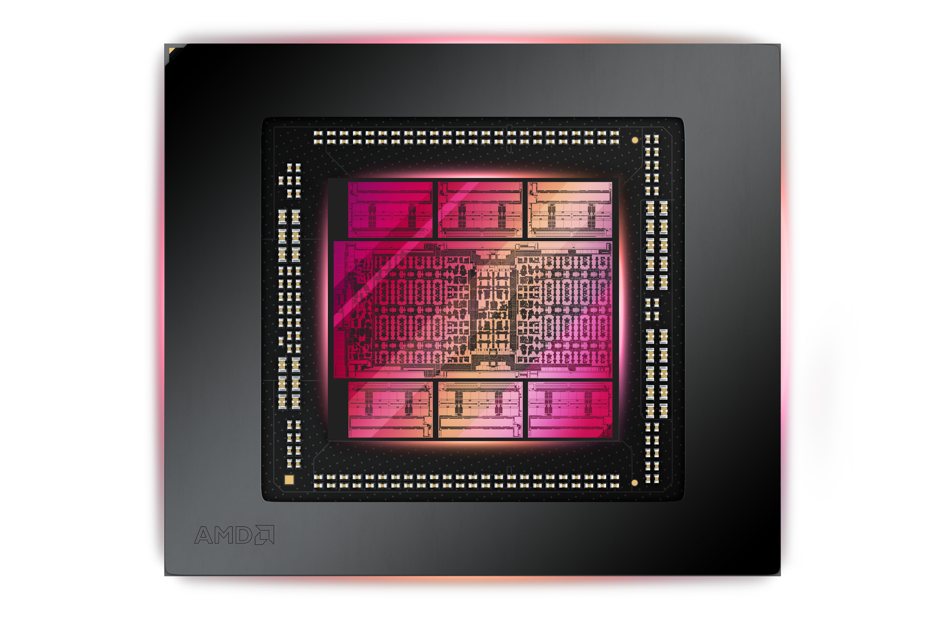
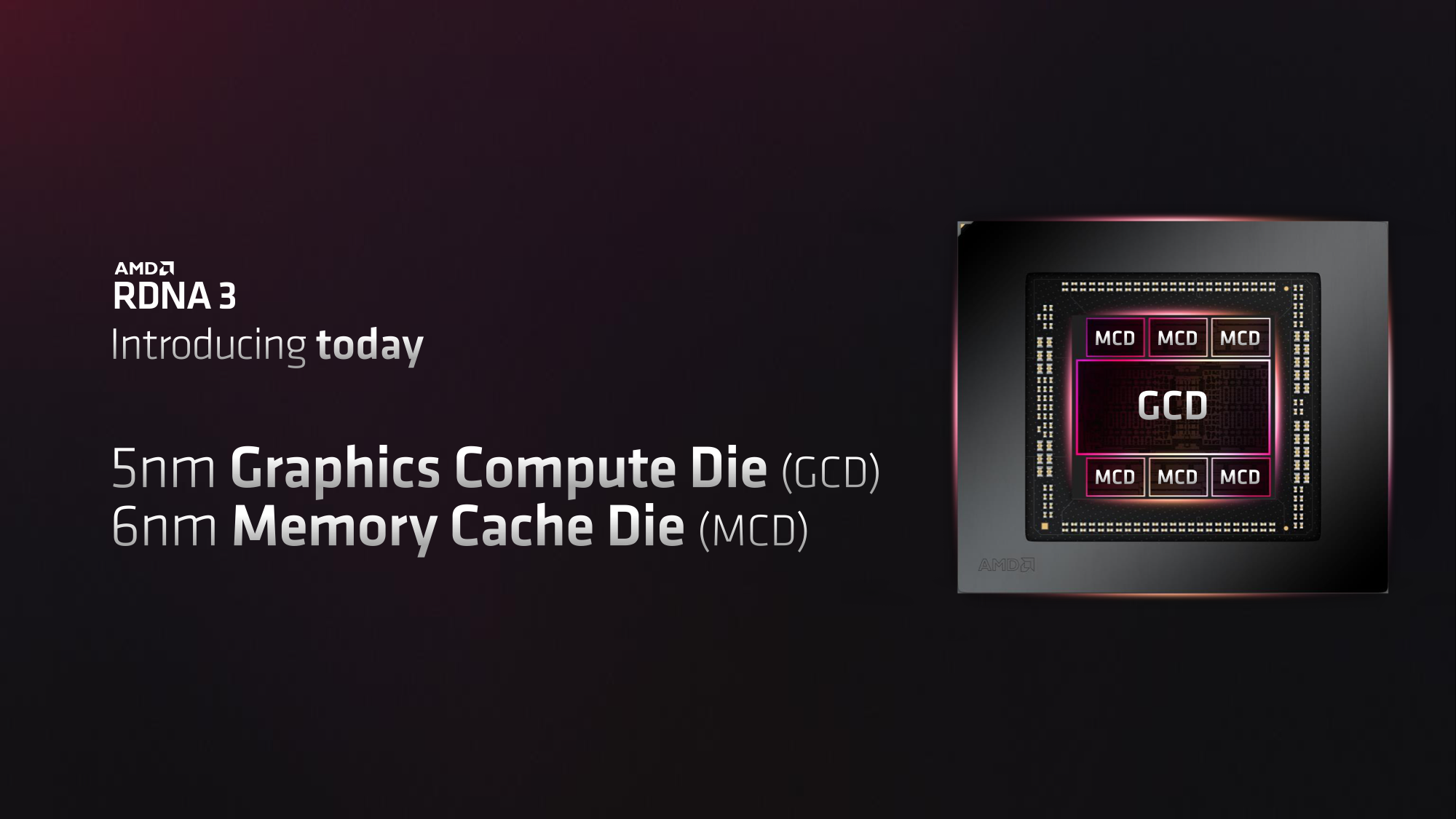
The two new graphics cards (their specs discussed in this article) that AMD announced yesterday are based on the Navi 31 GPU. We can no longer rally refer to it as a “chip” (although for simplicity’s sake, I suppose we will keep doing that), as AMD has now definitively confirmed that it is a chiplet solution combining 5nm and 6nm dies. In total, this multi-die assembly has 58 billion transistors.
The main part called GCD (Graphics Compute Die) is a 5nm die manufactured on TSMC process. Its die area is relatively small compared to Nvidia’s 4nm AD102 GPU with uts 608 mm², the Navi 31 GCD occupies just 300 mm². This is significant, as manufacturing costs should be significantly lower against Nvidia’s GPUs, allowing graphics cards to be sold at lower prices.
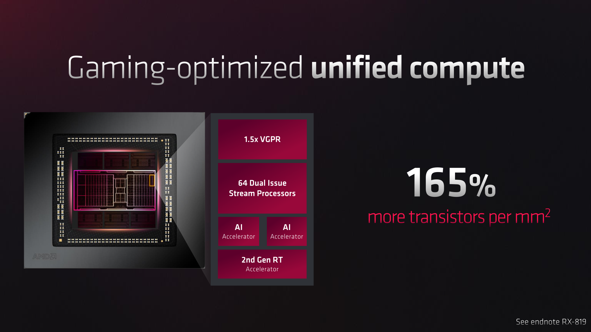
The GCD chiplet contains all the high-performance compute resources – in particular the CU blocks, but also the multimedia engines for multimedia processing and the video output block. The Navi 31 has 96 CUs in total, giving it 6,144 shaders (as to why so many, more on that in a moment).
Each CU block has four texture units (so 384 total), one ray accelerator (96 total), and two AI units (192 total). The 96 CU blocks are divided into six shader engines, with the entire GPU having 192 ROPs, so these appear to be linked to the shader engines (32 ROPs per SE).
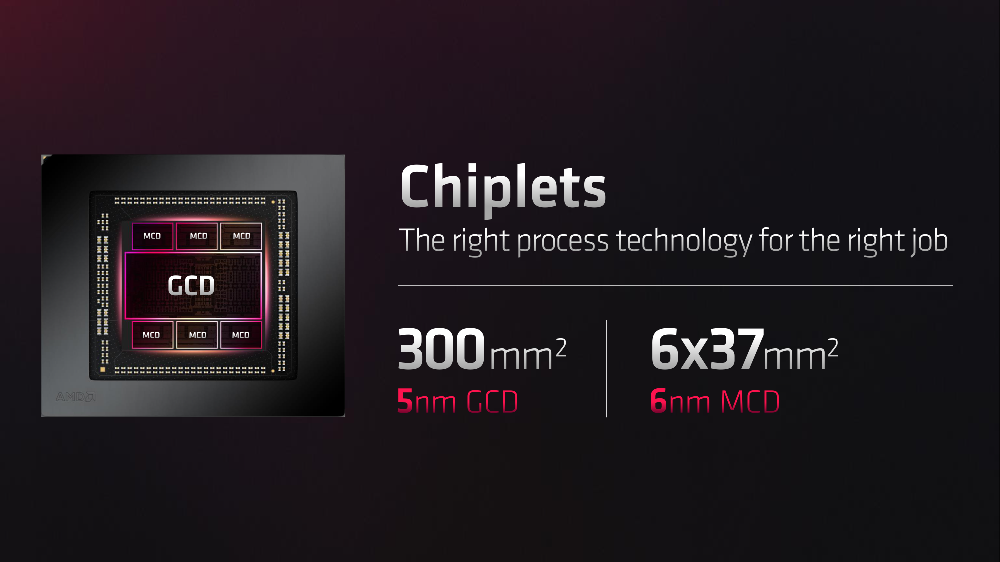
Six MCD chiplets are attached around the GCD (Memory Cache Die). These are manufactured using the cheaper 6nm process (also provided by TSMC). These chiplets are significantly smaller (37 mm²) and contain memory subsystem components – notably a GDDR6 memory controller with a total width of 64 bits per chiplet and a 16MB Infinity Cache block. Since there are six MCDs in Navi 31 chiplets, this adds up to a 384-bit memory bus and 96MB of second-generation Infinity Cache.
The MCDs will support faster memory than the RDNA 2 generation GPUs have – this first generation achieves an effective bandwidth of 20 Gb/s per bus bit, or as it is often simplified, an effective clock speed of 20.0 GHz.
Second-generation Infinity Cache
This 2nd gen Infinity Cache has a lower capacity than with the previous Navi 21 GPU (it had 128MB), but its actual utilization is said to be improved – even with the lower capacity, it should be able to hold data that the GPU repeatedly accesses more efficiently (according to AMD at least), so it should do a better job eliminating traffic to main memory and thus also reducing power consumption.
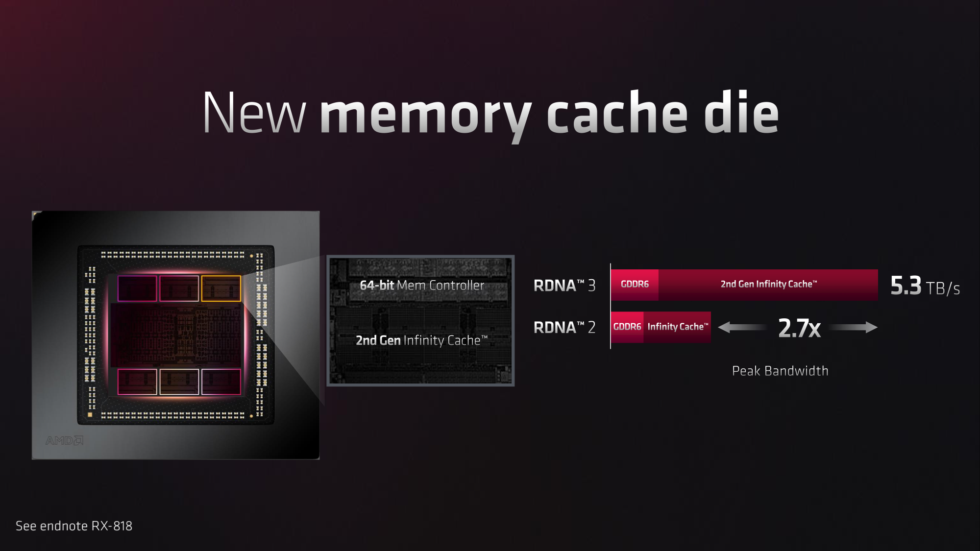
To make the Infintiy Cache work despite its detachment outside the main chip (note that it is the equivalent of the L3 cache in CPUs, where AMD has always kept it on the same piece of silicon), the MCD chiplets are connected via a very high-performance interface. The communication between GCD and MCD is said to have a bandwidth of up to 5.3 TB/s (that’s likely the aggregate bandwidth for all six interfaces together). The second-generation Infinity Cache in Navi 21 is said to deliver 2.7× better bandwidth than the first-generation Infinity Cache in Navi 21.
The interconnection of the GCD and MCD chipsets is reportedly implemented using Elevated Fanout Bridge technology, i.e. silicon bridges integrated in the substrate (which is a similar technology to Intel EMIB).
New CU architecture, 2× as many shaders
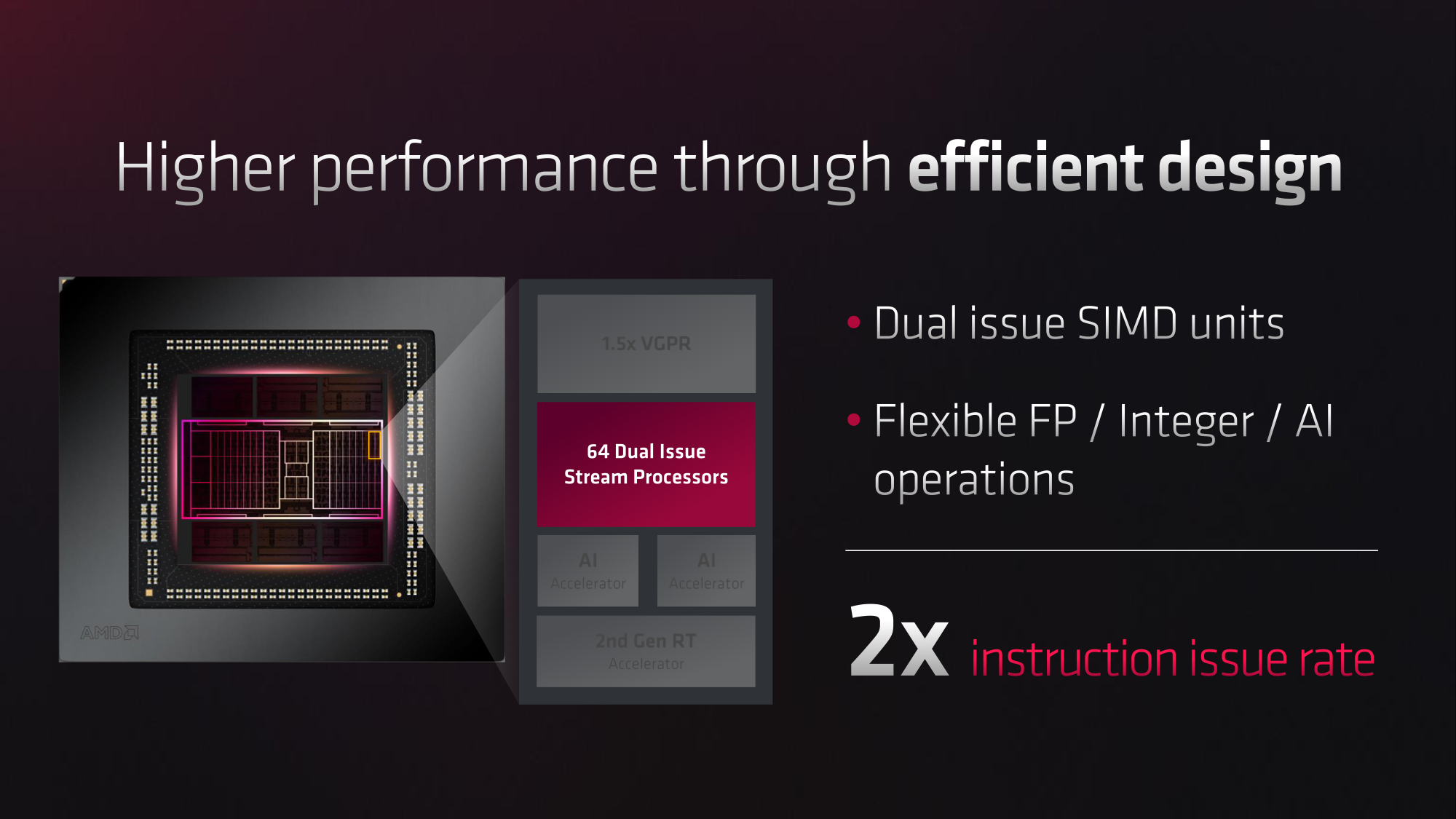
The compute units (CUs) of the RDNA 3 architecture are significantly redesigned. Since the first GCN architecture GPUs nearly 11 years ago, AMD’s GPU base block has always had 64 shaders (“ALUs”), although the implementation has varied over time – four 16-wide SIMDs for GCN, two 32-wide SIMDs for RDNA and RDNA 2.
RDNA 3 fo the first time gives the SIMD units (which provide those “shaders”, stream processors or also “shader ALUs” or “FP32 units” that are usually mentioned) the ability to process two instructions per cycle. So two 32-wide SIMD units should still be used, but with the “dual issue” capability they have a theoretical compute capacity of 128 shaders instead of the current 64. These two concurrently processed instructions can be of different types – integer and FP32, so it should be a flexible solution. However, this doubling of “ALUs” or shaders is done within the framework of a single CU structure derived from the previous generations, so 64 of these dual-issue shaders aren’t same as 128 shaders, since they share some control and compute resources that has only been serving only 64 shaders in RDNA 2 compute unit.
This change is broadly similar to how Nvidia’s Ampere GPU architecture doubled the number of FP32 units. This was already partially implemented in Turing, but there the second instruction could only be a less common integer op, not a floating-point instruction. But the stated number of shaders is derived from FP32 computations, which is why the doubled number of shaders only started to “count” in Ampere. Also, for Ampere, the 2× increase in the number of FP32 units did not lead to a 100% increase in the resulting performance (or at least not usually), and things should probably be similar for RDNA 3. So 64 dual-issue shaders in a RDNA 3 GPU will in practice be pulling less weight relative to the resulting performance compared to 128 shaders in an RDNA 2 GPU.
Anyway, this solution is supposed to be optimized for die area efficiency (see the small area of the Compute chiplet), which is probably the same reason that led not only Nvidia but also ARM (in the GPU architecture Valhall 4th generation) to a similar architecture concept.
12,288 or 6,144 stream processors?
Note: we aren’t yet certain whether the GPUs will now be stated to contain 128 or jsut 64 shaders per CU. Hardware sites seem to be opting for the former way, but AMD didn’t lean towards either form in the presentation and just lists CU counts (which also works if you get used to it, the CU count is comparable to Intel’s Xe Core count or the GPU core concept used by Apple). However, on their website in the specs pf the cards, AMD lists a figure of 6144 shaders for the Radeon RX 7900 XTX, so dual-issue is not accounted for. We shall see what counting scheme will ultimately prevail.

When Nvidia doubled the FP32 units in Ampere, apparently they were also undecided for a long time whether this should translate into the reported number of shaders (or as Nvidia says CUDA cores, which however is not accurate because the term core corresponds to a single SM block, like a CU does for AMD GPUs). Some card makers were said to have already printed materials with half the figures assuming 64 shaders per SM, so it looks also Nvidia may have decided to count 128 shaders per one SM almost at the last minute time.
Update: the notation settles on 64 shaders per CU
In the end, AMD has decided against counting each CU as 128 shaders / stream processors / FP32 units, which Nvidia did. This means that the specs of all RDNA 3 will only show half as many shaders as expected originally. Navi 31 is therefore just 6,144 shader units and not 12,288. However, this only a cosmetic change that doesn’t alter anything in the capabilities of hardware.
It also means that if you consider the RDNA 3 CU to be 64-wide (but actually capable of double the ops), it will appear to have improved performance per clock compared to truly 64-wide RDNA 2 CU. Basically, it will look like the architecture has improved “IPC”. On the other hand, Nvidia’s counting Ampere and Ada SMs as 128 shaders means that the apparent IPC per 1 shader seems to be lower. Again, this is just a cosmetic difference that doesn’t matter in any way in practice. The “IPC” change needs to be judged based on a single SM or CU in these cases.
AI units
A potentially very important change is that RDNA 3 should have better performance in AI acceleration. It’s not entirely clear if RDNA 3 provides separate execution units for AI within the CU, or if it’s referring just to a separate mode that still uses the same ALUs that execute FP32 shaders (i.e. something similar to how the same CPU pipeline can compute SSEx and AVX/AVX2 and VNNI/256 instructions). So two AI units per CU would correspond to two SIMD pipelines in the CU and share more or less resources with them.
In any case, these AI accelerators share the same schedulers, registers, and other resources that regular shader ALUs use (but we think this should in part apply to Nvidia and Intel’s architecture as well). Therefore, this AI acceleration won’t result in some order of magnitude performance boost, but at the same time adding it isn’t too much of a cost in chip area and power consumption.
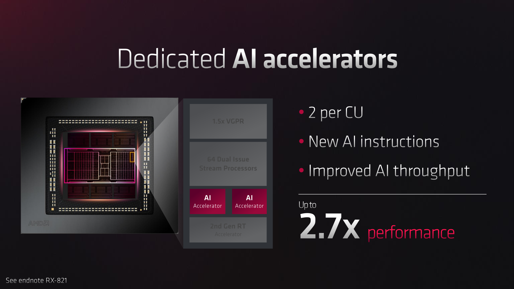
According to AMD, using these units can achieve 2.7× higher performance. But this is a comparison of Navi 31 and Navi 21 and this performance increase is also due to the higher number of CUs (96 instead of 80) and higher clock speeds. In terms of “IPC” the increase is only 2× courtesy of RDNA 3 being able to process twice as many BFloat16 operations per CU, but this is merely proportional to the 2× increased number of FP32 operations possible per cycle per CU due to dual-issue. From this, it seems that there are no particularly special matrix units dedicated to AI acceleration as in the CDNA and CDNA 2 architectures. The question is whether to talk about AI units at all, even though they are on the CU diagram.
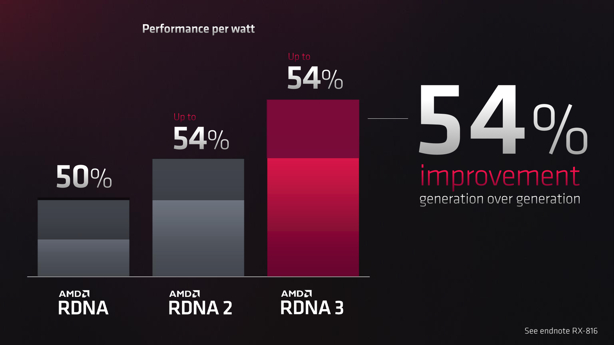
Energy efficiency up 54%, transistor density up 165%
A significant change in the RDNA 3 CU architectures is the increase of the physical register file that the CU operates with by 50 %. These registers appear to be utilised by shaders, ray accelerators for raytracing computation as well as for AI acceleration. This resource sharing is said by AMD to be one of the main conceptual features of the RDNA 3 architecture with the goal to make the most efficient use of a given area of silicon.
The RDNA 3 architecture is apparently designed to achieve very high transistor density, with 165 % more transistors per square millimetre than RDNA 2 on the 7nm process. This is a much larger increase than the transition from 7nm to 5nm process alone would allow. In the RDNA 2 architecture, a CU pair had 215 million transistors in a 4.33 mm² area, while in RDNA 3 a CU pair has 331 million transistors in just 2.50 mm².
AMD states that the goal with RDNA 3 was to improve power efficiency (performance per watt) by 50 % over RDNA 2, which was publicly announced long in advance. In the end, it’s more than that, with AMD’s measurements suggesting an improvement of up to 54 %.
More powerful ray accelerators for ray tracing
The ray accelerators have already been mentioned, i.e. the units responsible for hardware acceleration of raytracing effects analogous to Nvidia’s RT cores, which were first used in RDNA 2 GPUs. In RDNA 3, they also have an improved architecture, their performance is supposed to be 50 % higher per CU and they are supposed to handle 50 % more rays at once.
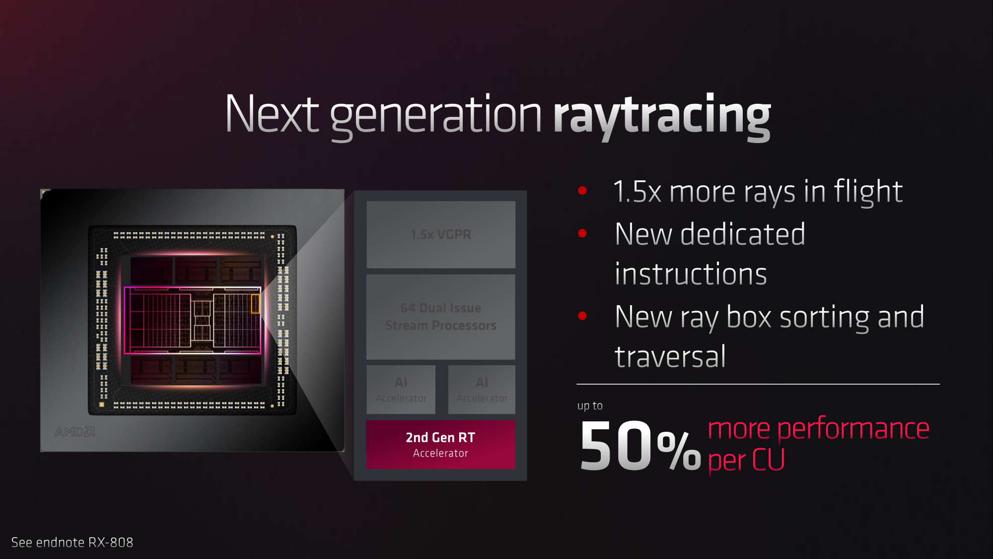
Ray accelerators have various improvements in sorting and analyzing the “boxes” used during raytracing calculations using the BVH (Bounding Volume Hierarchy) method used in today’s raytracing games. But even generic shaders, which do some of the work in these calculations not relegated to dedicated RT units, have some new instructions to improve raytracing performance, according to AMD.
Higher clock speed for frontend, lower for shaders
An interesting change is that the shaders will run at a different clock speed compared to the frontend in RDNA3-based GPUs. AMD says that according to its analysis, the GPU frontend, which distributes instructions to compute units, is more often than not the limiting factor. RDNA 3 has therefore decoupled them, with the frontend running asynchronously at a higher clock speed – or perhaps it’s better to say that the shaders run at a reduced clock speed, thus improving power efficiency (and extracting more performance from a given TDP allocation).

For Navi 31, AMD reports that the frontend runs at 2.5 GHz (15 % faster), while the shaders run at 2.3 GHz, saving about 25 % power. It seems that these particular values could apply to the Radeon RX 7900 XTX. By the way, that 2.3 GHz figure for shaders is still 15 % more than what the 7nm GPU of the RDNA 2 architecture went to market with, according to AMD.
Elsewhere in the presentation, AMD states that RDNA 3 achieves 18 % higher clock speeds than RDNA 2, but it’s probably better to wait for real-world gaming data from independent tests to determine whether clock speeds have actually improved and by how much.
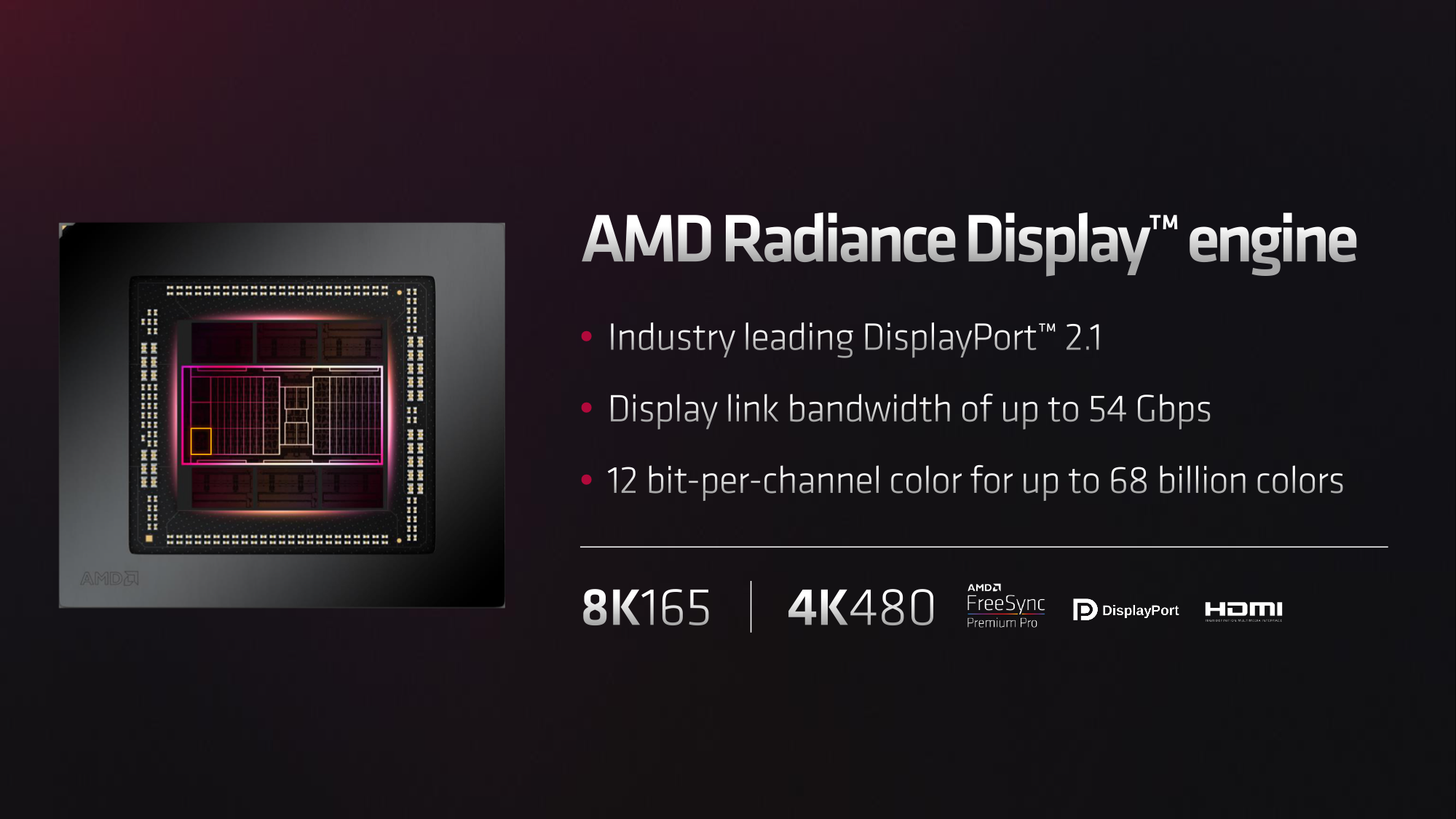
New Display Engine, new Media Engine
In addition to the new RDNA 3 compute and graphics architecture, these GPUs also feature new blocks for display output and multimedia. The display output is handled by a component called the AMD Radiance Display Engine. Its main new feature – and one that Nvidia’s new generation of GPUs doesn’t have an answer for (beyond Nvidia’s claim that nobody needs it) – is DisplayPort 2.1 output support. As a result, AMD promises significantly better support for new high-resolution and high refresh rate displays.
8K at up to 165 Hz, 4K at 480 fps with DP 2.1
The Navi 31 and Radeons based on it support 4K (3840×2160 pixels) resolution at up to 480 Hz thanks to this output block and DisplayPort 2.1, and can handle 8K (7680×4320 pixels) resolution at up to 165 Hz (and can do this with HDR colours at 12 bits per channel). At 2560×1440 pixels, up to 900 frames per second is said to be possible, but here the usefulness already seems quite questionable. We’ll see if any such monitors ever appear.
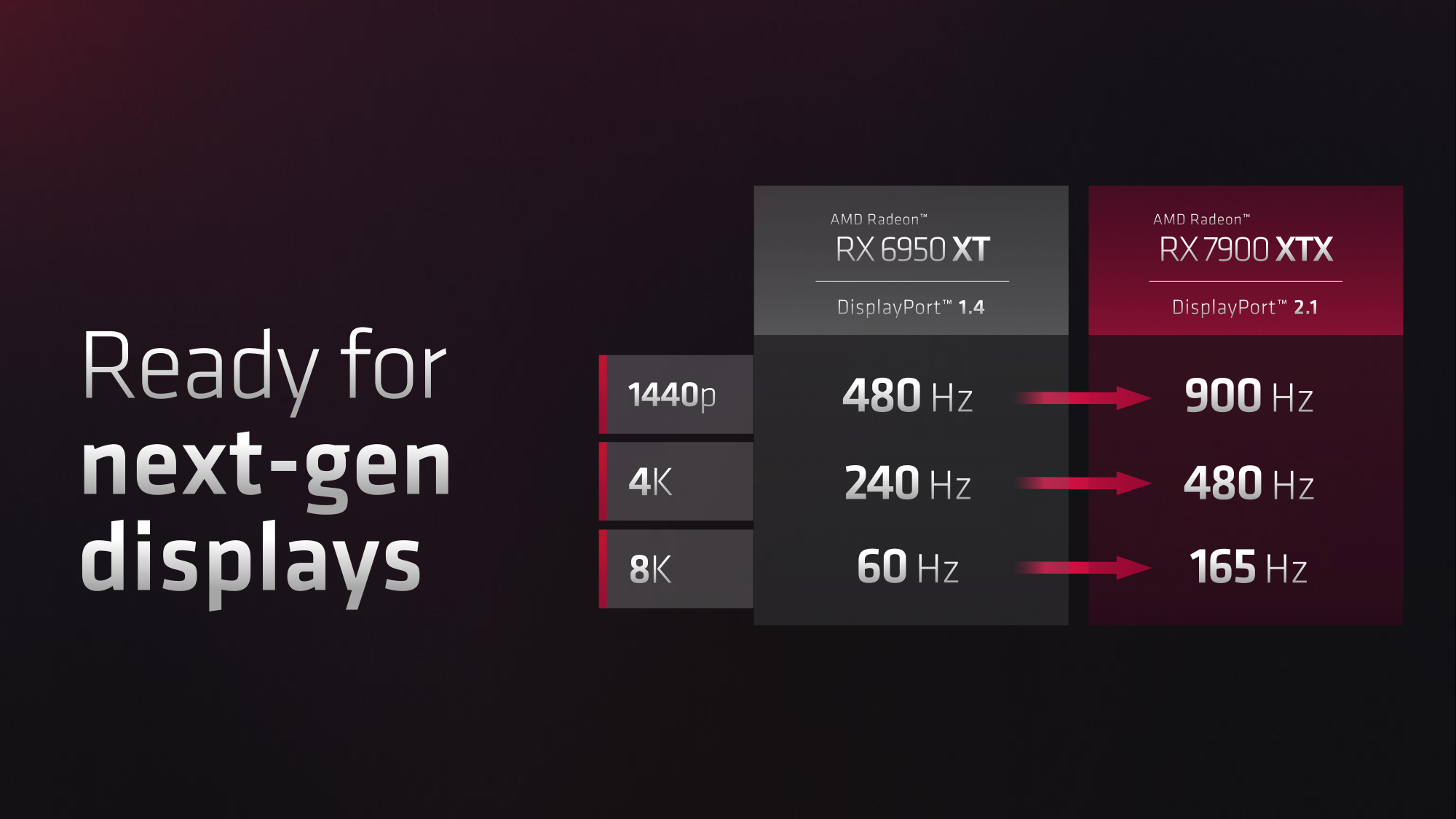
The maximum supported bandwidth when communicating via DisplayPort 2.1 is 54 Gb/s according to AMD (but more accurately it should be 52.2 Gb/s for image data, 54 Gb/s is before overhead is subtracted), which should mean that a UHBR 13.5 subset with four 13.5 Gb/s lanes is supported. There is also UHBR 20 with 20Gb/s lanes that achieves a bandwidth of 77.37 Gb/s, but this will probably not be implemented until the next generation. AMD should be a bit ahead of Intel Arc graphics with UHBR 13.5, since Intel’s implemenation only supports DP 2.0 (but should also support DP 2.1) with just UHBR 10, which means 10 Gbps lanes and a slightly lower maximum bandwidth of 38.69 Gbps.
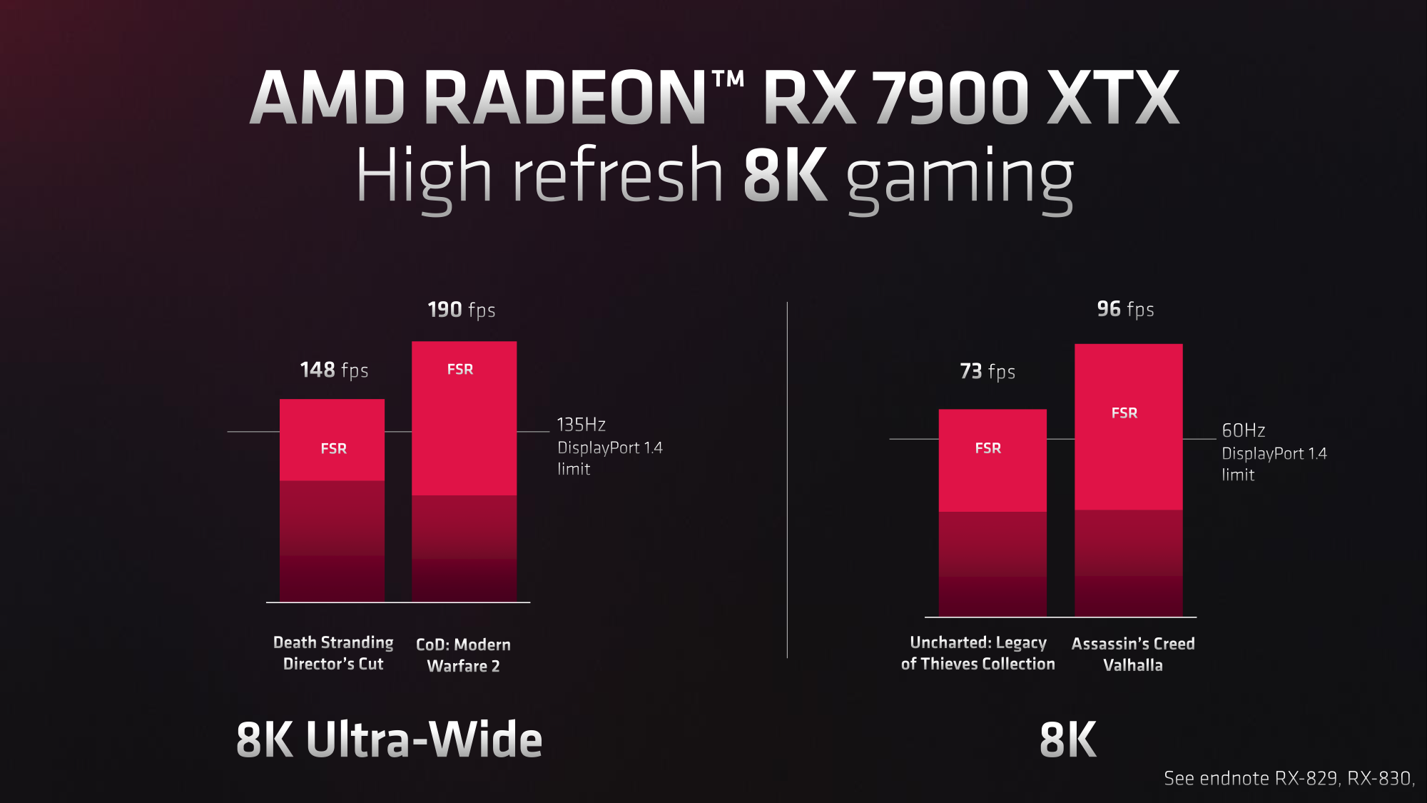
But even that still gives better optcapabilities than the GeForce RTX 4000 have, as Nvidia settled for just DisplayPort 1.4a with those. That provides a bandwidth of 25.92 Gb/s which isn’t even enough for 4K at 120 Hz without lossy compression. These Nvidia cards have 8K resolution at 60 frames per second as an absolute limit. That’s far from ideal if you want to last a few years with this generation of graphics cards – there will soon be monitors on the market that they won’t be able to run at their maximum clock speed, but the Radeon RX 7900 XT and RX 7900 XTX will.
As AMD pointed out, with FSR/FSR 2.0 upscaling, you can already run into and above the 60Hz (FPS) limit with new graphics even at 8K resolution. In the demo shown, the Radeon RX 7900 XTX was able to produce 96 FPS in Assassin’s Creed Valhalla Dawn of Ragnarok and 73 FPS in Uncharted: Legacy of Thieves Collection.
In addition to DisplayPort 2.1, HDMI 2.1 is of course also supported, as well as USB-C video outputs (which should use the DisplayPort signal). On AMD’s reference cards, according to the renders, there are a pair of DisplayPort 2.1s, one HDMI 2.1 and one USB-C.
AV1 encoding and decoding in 8K at 60 frames per second
Navi 31 also has a new multimedia engine with hardware video encoders and decoders. Or rather, there are two engines in the GPU, so two independent encoding or decoding streams can be processed simultaneously. The supported formats are H.264, HEVC and AV1, for which not only decoding (which RDNA 2 graphics were already capable of) but also hardware encoding (compression) to this format is now supported, a new feature also brought by GeForce RTX 4000 and Intel Arc generation Alchemist graphics.
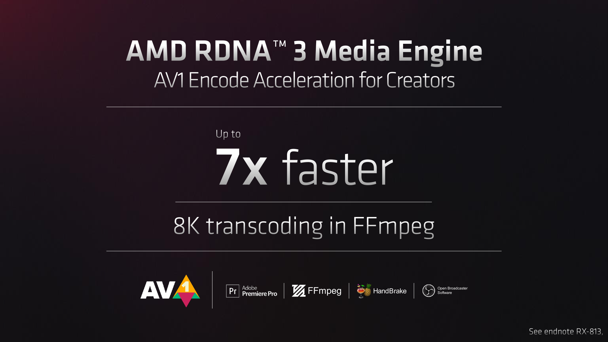
AV1 can be encoded and decoded at up to 8K resolution at 60 frames per second, and the multimedia block also supports the use of various AI-based post-processing filters. The multimedia engine, by the way, is said to run at a clock speed 80 % higher compared to RDNA 2 architecture chips.
SmartAccess Video
AMD also talked about a new SmartAccess Video feature in their presentation, which is apparently unrelated to the PCIe Resizable BAR used in games. It should apparently be about using the processor (or possibly its iGPU) during video encoding and decoding to improve the performance of hardware encoding and/or decoding. It can reportedly improve performance by up to 30 %, especially in situations where multiple streams are processed simultaneously so that two multimedia engines are already saturated (AMD talks about parallel “multi-stream transcoding”).
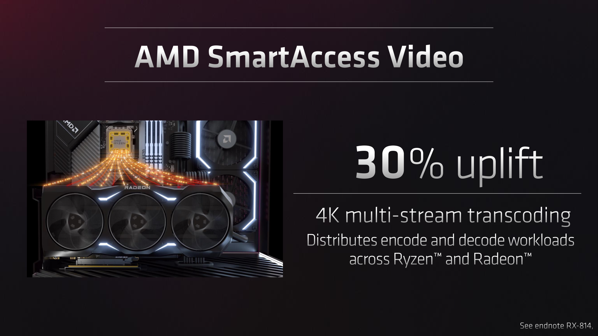
But this feature is apparently exclusive to PCs with both the Radeon RX 7000 generation and the Ryzen 7000 processor. It should be available in various software applications like OBS, Premiere Pro, but also FFmpeg and others.
Some unknowns remain
These are not likely to be the only changes and innovations that the RDNA 3 architecture brings, there’s likely more under the hood as usual. Further details are probably yet to come. For example, nowhere in the presentation did AMD mention whether the Navi 31 GPUs and with them the Radeon RX 7900 XTX and Radeon RX 7900 XT support PCI Express 5.0 for connection to the system, or whether they will stay with PCIe 4.0 like Nvidia Ada.
So far it looks like PCIe 5.0 is not happening. At least according to ComputerBase only PCI Express 4.0 ×16 is still supported. This would be another rumor that didn’t come true (besides high, >3 GHz clock speeds that were unofficially expected), although the leakers were right about the number of units or Infinity Cache capacity and chip size). So there may still be some surprises to come.
Sources: AMD, AnandTech, ComputerBase
English translation and edit by Jozef Dudáš