

Golden Cove Architecture: highest-performance Frontend in the history of x86 cores
Intel’s Alder Lake CPUs are poised to be the biggest hardware event this year. Intel has unveiled the core architecture of these CPUs and we have analysed the details and new improvements inside. There’s promise of huge performance and one of the biggest architectural leaps in x86 processors, for the first time with six parallel decoders and further IPC increases, showing Intel taking the same path as Apple’s highly effective cores.
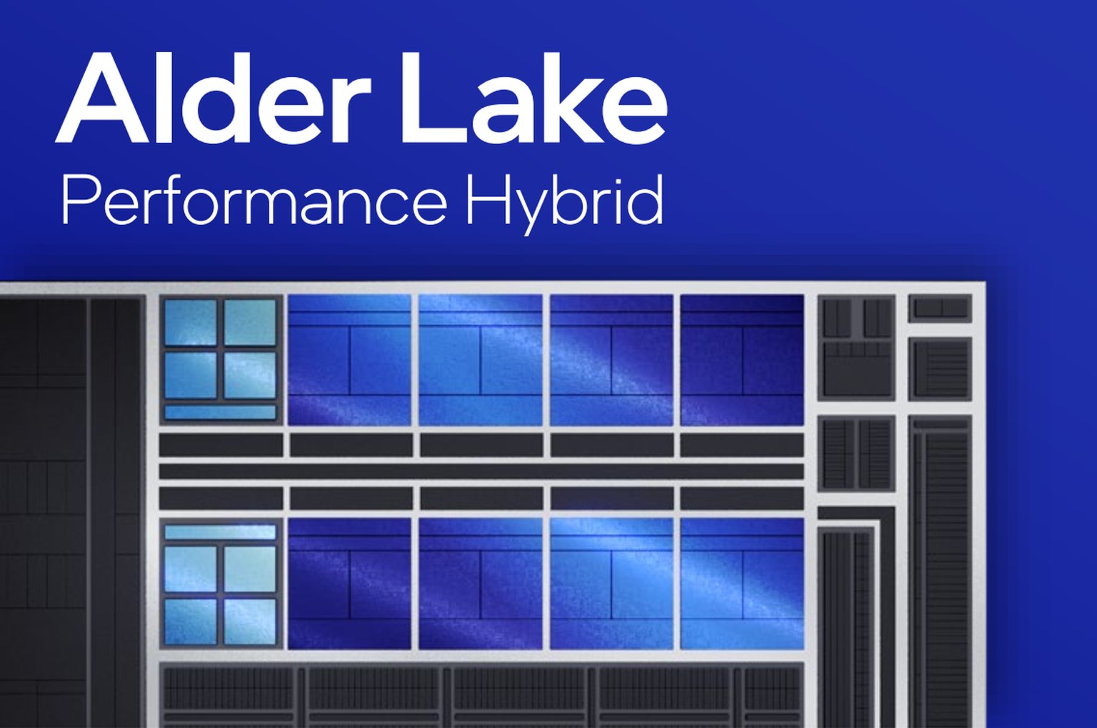
It has long been known that Alder Lake is moving to the “big.LITTLE” concept, combining together cores of higher and lower (but more energy-frugal) performance. Intel has released information about both the so-called “big core” and the “little core” which will provide boost in multi-thread performance (and second as a more energy-efficient core for running less demanding background tasks, etc.).
But first, let’s talk about the big core. Intel now officially calls it “Performance Core”, or P-Core (while it has been codenamed Golden Cove in the past), and its role is to achieve the highest possible single-threaded performance, a parameter that determines the performance of many common applications and also system responsiveness.
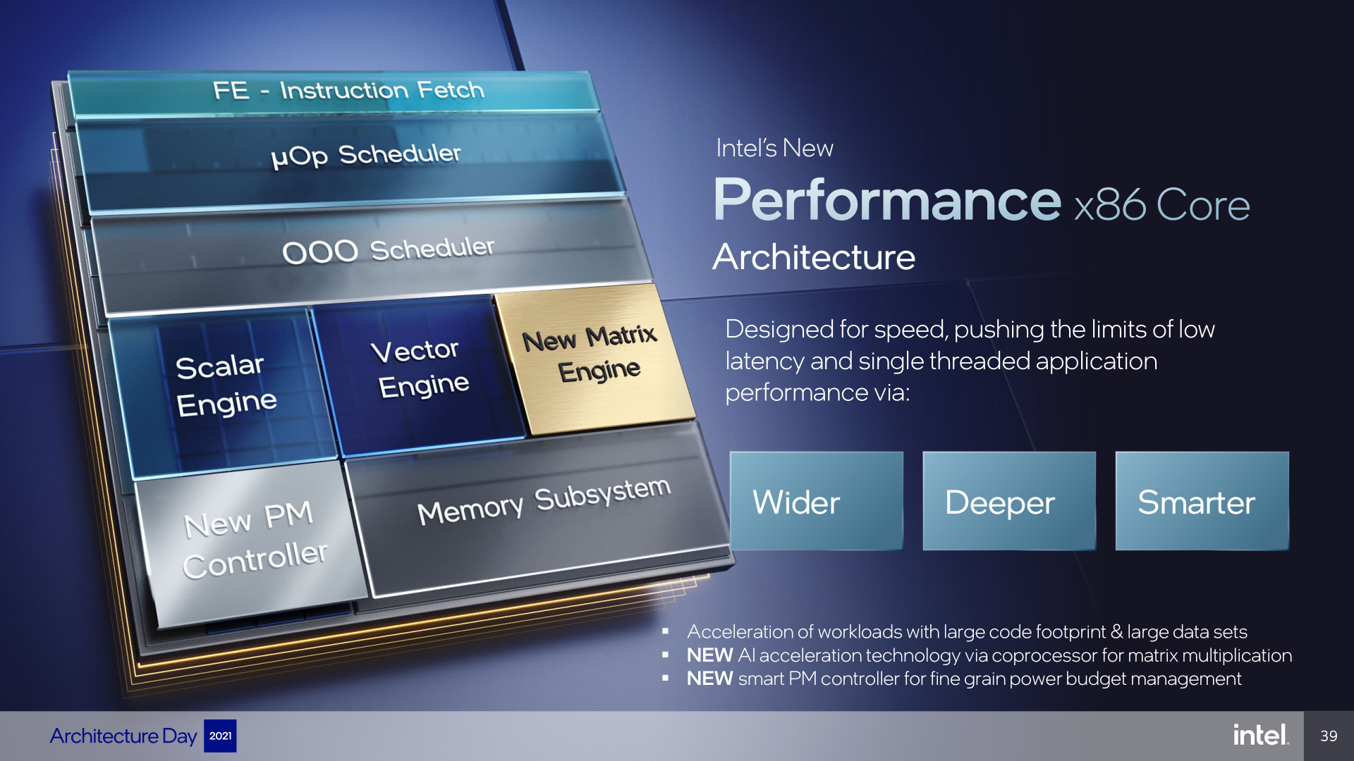
Golden Cove could finally satisfy those complaining Intel allegedly hadn’t introduced anything truly new in a long time, and all the individual cores from 2011’s Sandy Bridge are still more or less variations of the same. Golden Cove brings forth an architecture that is actually still based on their DNA (but so is the case with all architectures today), however its basic blocks have been redesigned and in all substantial parameters and the result is a much larger and higher-performing core. It significantly widens and deepens the out-of-order engine to reach higher IPC and the leap in performance should be very large. According to Intel, it even represents the largest upgrade of Core microarchitecture in the last decade, which would put Golden Cove (and Alder Lake processors) in a similar position as the mentioned Sandy Bridge architecture.
Golden Cove follows the concepts of the previous “big” 10nm Sunny Cove/Willow Cove core, it is functionally similar due to HT support, i.e. simultaneous processing of two threads on one core. This allows a core to improve performance in multithreaded code by making better use of the core’s computing resources.
The Golden Cove core should also achieve a similar if not higher clock as what we saw with the Rocket Lake or Tiger Lake chips, because it uses a more advanced Intel 7 manufacturing process (formerly known as 10nm Enhanced SuperFin).
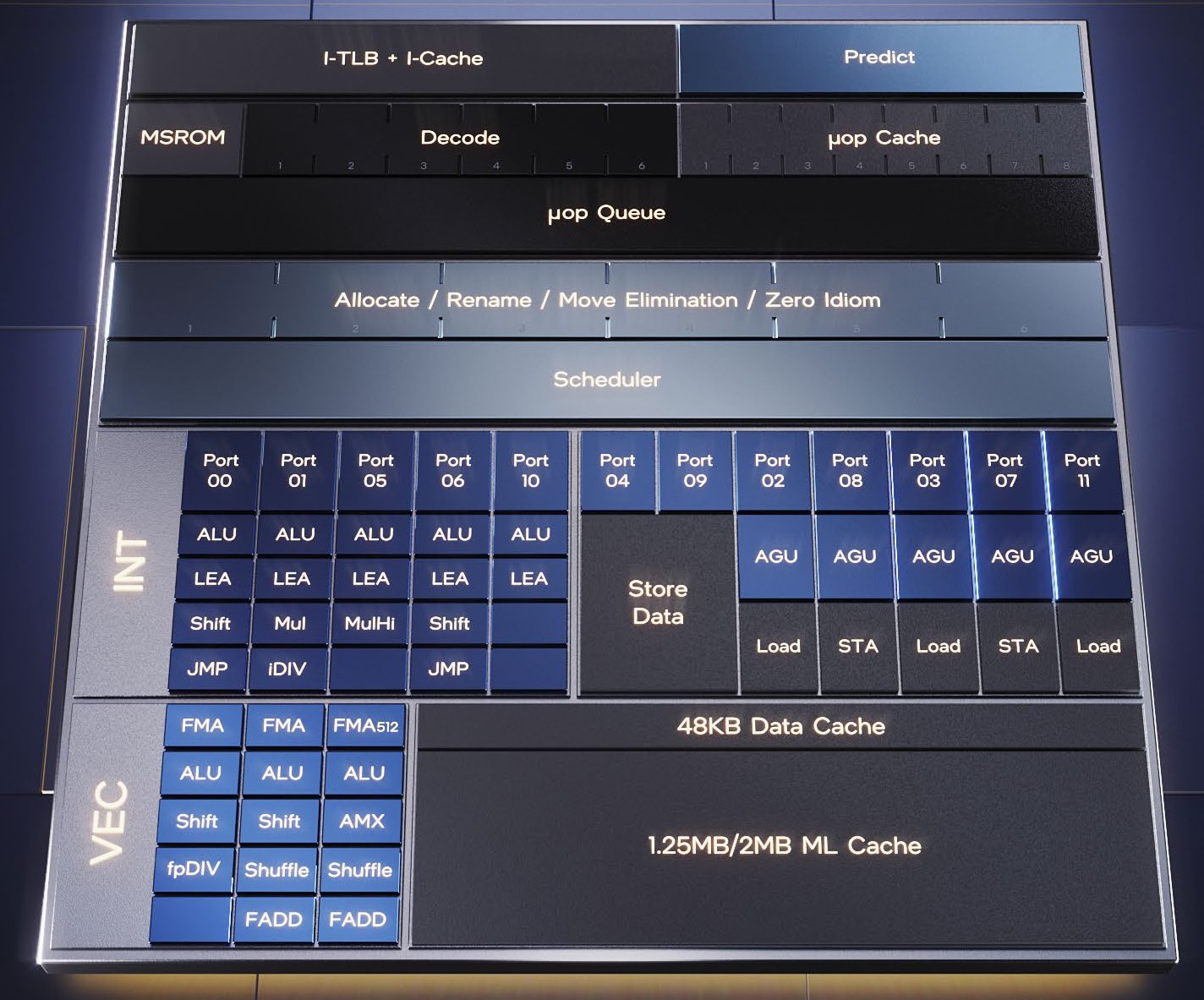
Overall, Golden Cove increases and enhances most resources inside the core, and the architecture could somewhat be compared to the concept that Apple is pursuing, including increasing the number of ALUs in the core. However, the ALUs themselves are something that comes into the picture more towards the end of the working path through the processor core, so we will start the description of the architecture in the so-called Frontend instead, where the route of instructions/computing going through the core begins.
A core busting myths about the fundamental limits of the x86 architecture?
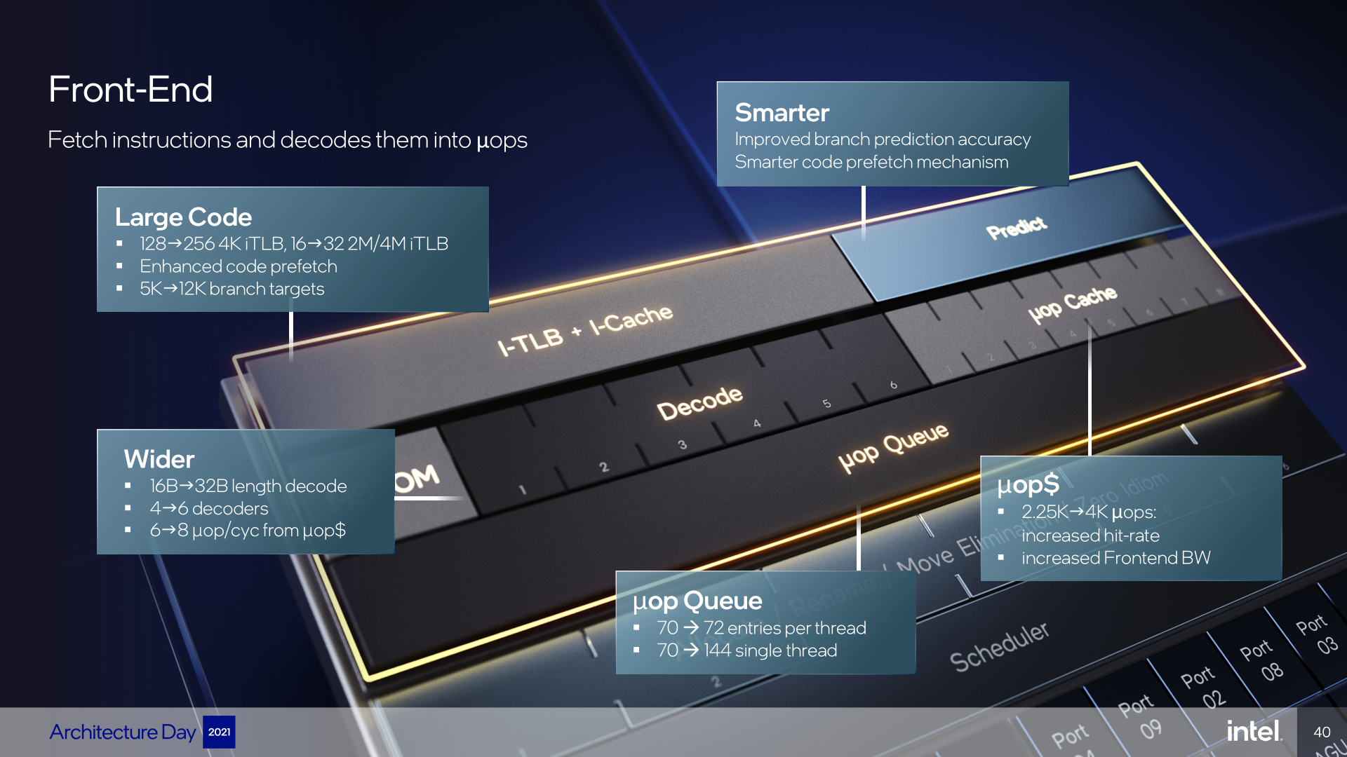
The Frontend is where the most fundamental or perhaps the most symbolic change took place: Golden Cove increases the core “width”, meaning how many instructions can be processed in parallel in one cycle, right here at the beginning. Since the Conroe/Core 2 architecture, Intel cores have had four decoders, so they could process up to four instructions per clock in the decoding stage. More than ten years ago, Sandy Bridge added the μOP cache that caches decoded instructions, which allows bypassing the decoders if the core finds the necessary instructions in this cache (this increases performance, but the second purpose is to reduce power consumption), but otherwise the limit of four decoders has remained—until now.
Intel has expanded the number of decoders to six in Golden Cove, so the core is now “6-wide” and will be able to decode up to six instructions per cycle. Only Apple has a wider decoding now, with the Firestorm core in the M1 and A14 chips already being 8-wide, while the Zen 3 from AMD is still 4-wide. Golden Cove’s ability to decode six instructions will probably have some limitations Intel has not revealed yet, where so-called complex instructions will have this bandwidth reduced, because they will be processed only by some of the decoders (“complex decoder”), while most (“simple decoder”) could process only more common instructions. Complex instructions are typically those that produce more than one μOP in further processing.
The price for extending the decoders is probably the extension of the pipeline by an extra stage, which probably helped to enable this extension (because the decoding was divided into more pipelined steps). This can be seen in Intel’s information that the penalty for misjudged branching has increased—from 16 to 17 cycles.
The x86 architecture will not allow more than four decoders…
This is also interesting because in the context of Apple’s ARM processors with very wide cores (but low clock rates), we have heard lots of opinions recently that a similar architecture is possible only with ARM and not in x86 instruction set processors, because their instructions are variable-length (and raise some other complications). Particularly confident of those opinions went as far as alleging that more than four decoders in x86 is near to impossible to have.
This topic is probably so popular also because where x86 cores differ from ARM, is exactly in the frontend part up until and including the decoding phase; after that the differences fade as decoded μOPs that are processed in the rest of the pipeline onwards can be pretty similar between ARM or x86. The “x86 limitation” in the decoding phase was therefore taken as a core argument for the notion that the x86 architecture has no future and there’s a need to move to ARM. However, it seems that Intel might now prove this point wrong by using six/6-wide decoders in the Golden Cove architecture. Although we still have to wait until we see the result and can be sure the x86 complications will not turn out to be relevant here after all. We’ll have to see whether, for example, the 6-wide leads to disproportionate power consumption.
Along with strengthening the decoding stage, Intel has extended the previous stage of processing, the so-called Fetch stage, which reads code (i.e., the instruction stream) from the instruction L1 cache of the processor and passes it to the decoders. Here, too, Intel had significant limitations for a long time, Fetch would for long only read a maximum of 16 bytes per cycle. Basically this has been the case since the Pentium Pro from 1995. Some x86 instructions can be very long (up to 8 bytes), so this could sometimes be a limitation even for a 4-wide core (but this limitation can be bypassed by the μOP cache togoether with the decoding limit). For the first time, Fetch has been doubled and delivers 32 bytes of code per cycle in Golden Cove.
It should be noted that based on software profiling, the performance of core (or IPC) in applications typically does not reach four instructions per cycle at all. Often the usual programs are closer to an average of one instruction per cycle than four or six. This is because of branching, waiting for data from memory, or because dependencies of one instruction on another make it impossible to execute multiple instructions at once. Therefore, only four decoders in previous CPUs were not necessarily a performance bottleneck as drastic as it might seem. But extending this stage will allow performance to be increased in those cases/moments in your code where the potential for greater instructional parallelism does exist. And to eventually raise the IPC above a certain level, this expansion likely has to come at some point—Intel has apparently decided that the time is right now.
μOP cache, instructional L1 cache
Intel has kept the instruction L1 cache capacity the same as what the older cores (and also AMD Zen 2/3) have, it is only 32 KB—compared to 192KB capacity in the Apple Firestorm core. However, the L1 TLB (Translation Look-Aside Buffer) for instructions has been enlarged to 256 instead of the previous 128 entries and 32 instead of 16 entries for large (2MB/4MB) memory pages. Prefetching to the L1 instruction cache is also improved.
Hand in hand with the decoder improvement, the μOP cache for already decoded instructions has also been enhanced. Previous Intel cores (or AMD Zen/Zen 2) could supply up to six instructions per cycle from the μOP cache, which the Golden Cove expands to 8 μOPs per cycle (AMD Zen 3’s μOP cache has the same capability).
Same as its predecessors, the core architecture assumes that most of the time the execution path of instructions will not actually go through the decoders due to the necessary instructions (already decoded to μOPs) being instead found and sourced from the μOP cache. When operating from μOP cache, the decoders can be turned off (clock-gated) to save energy. According to Intel, the core should typically use the path through the μOP cache in about 80% of the execution time, so this is the primary case and the full-decode path is the less likely scenario.
At the same time, the capacity of μOP cache has also been increased, so the chance that the processor will find the instructions here and will not have to turn on the decoders (so-called hit-rate) increases. And the larger capacity allows significantly longer code loops to fit in the cache. While Skylake had a capacity of 1,500 instructions and Sunny Cove/Willow Cove/Cypress Cove increased it to 2,250, the Golden Cove core has increased the capacity to 4,000. AMD was a bit ahead in this regard, Zen 2 already has the same capacity and Zen 3 keeps the same capacity too).
The μOP Queue following the μOP Cache has also been slightly increased, with 72 instead of 70 entries for each of the two threads that the architecture can process (Golden Cove supports HT a.k.a. SMT, and one core processes two threads at once). What is new here is the ability to combine these separate queues for each thread into one with 144 entries if the processor processes only one thread instead of two.
The μOP Queue is followed by the Allocation and Rename phase, in which working registers are allocated for μOPs and the architectural registers are renamed (substituted for others from the physical register file) to eliminate conflicts. Also, this pipeline stage allows processing six operations (μOPs) per cycle, while previous Intel architectures could do a maximum of five. Here you can see how virtually all processing phases have been modified for higher IPCs in this core.
Performance should be further enhanced by Intel improving the processor’s ability to resolve conflicts at this stage and eliminating more instructions that do not need to be sent to compute units and are already resolved here. At this stage, the CPU eliminates MOVs (in Alder Lake perhaps it should work again, while Ice/Tiger/Rocket Lake had erratum and required a microcode update that turned this feature off) and other instructions that do not require the use of an execution unit. Another case of eliminated instructions are, for example, zeroing idioms such as XORing the same register in order to zero it (because this operation does not depend on the previous value of the register), the elimination of which the processors have been capable of for a long time. Golden Cove is capable of eliminating more instructions like this, but Intel does not say exactly how the capabilities have improved in this direction.
Significantly improved branching prediction
Before we look at the next part of the core, where out-of-order optimization of instructions takes place and then their execution, it is necessary to mention the branch predictor, which is in the frontend and operates early in the pipeline of instruction processing.
This part of the processor is always tuned continuously by microarchitecture engineers, so it should be improved in each new generation of CPUs (unless it is a “refreshed” silicon taking over core from the previous generation without changes). In Golden Cove, however, the prediction is said to be improved greatly. The accuracy (success rate) of predictors was improved by itself, but at the same time they also have much more memory available for their use, which should further improve the prediction, because the predictor has more data/information available. The L2 Branch Target Buffer (BTB) now has a capacity of 12,000 entries compared to 5,000 for the previous generation of architecture (for comparison, Zen 3 should have 6,500 entries).
The article continues in the next chapter.
- Contents
- Golden Cove Architecture: highest-performance Frontend in the history of x86 cores
- Expansion in computing units and expansion of the „window“
- FPU & SIMD units: AMX for Xeons, AVX-512 is dead in Alder Lake
- Fruits of wider core: 19% better performance per MHz