


New manufacturing process 8N: Samsung technology enhanced especially for Nvidia
In terms of hardware, September was a green month with the release of the new generation of Nvidia GPUs, GeForce RTX 3000. They are based on the new Ampere architecture. In this article we are going to discuss what’s new compared to Turing: the new SM architecture doubling the number of shaders, the manufacturing process and the characteristics of the two chips that have been unveiled so far.
Everything is new: manufacturing node, architecture, memory and connectivity
Ampere is a new generation of GPU in all aspects. It combines three innovations: a new manufacturing node, a new architecture of the blocks and GPUs, but also a new GDDR6X memory technology which differs from predecessors by using more efficient PAM4 signaling. We have already covered GDDR6X here so we’ll refer you to that writeup and skip it in this article.
Manufacturing node: custom modified 8N technology
It has been known for quite some time that Nvidia will start manufacturing GPUs at Samsung instead of TSMC, which is the most established of the silicon manufacturing foundires. Nvidia has already used Samsung’s 14nm process (14LPP) for some less powerful Pascal chips (GP107 in GeForce GTX 1050/1050 Ti). So when there were reports last year that Nvidia would use Samsung’s process for next-generation chips, it was first thought that it would be something similar.
In the end it turned out quite differently. Nvidia actually produces the most powerful GPUs, GA102 and GA104 units, at Samsung and only the computing GA100 die for servers is manufactured on TSMC’s 7nm process. However, the gaming Ampere is specific not only because it is from Samsung, but also because it is not 7nm. Nvidia has chosen an older Samsung technology, the so-called 8nm process, which is an improved version of 10nm process node in fact.
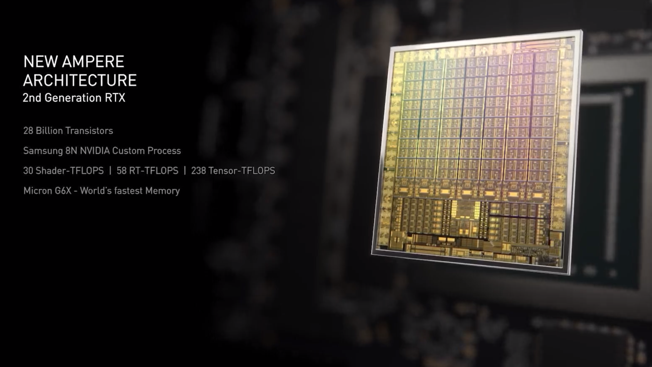
The process is called 8N because it is specifically designed for Nvidia’s use and should include various unspecified improvements and modifications. It should therefore be a better technology than the 8LPP process used by some mobile phone SoCs. According to some sources, modifications done for Nvidia result in up to 10% higher performance (meaning higher frequency could be achieved) than the original version of the process that was focused more on mobile SoCs. However, this process probably achieves lower energy efficiency and transistor density than the real 7nm process, which in the case of Samsung is employs EUV lithography. It’s likely that the 8N process is also inferior to TSMC’s 7nm node.
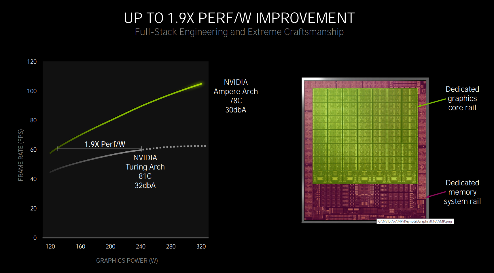
Nvidia reports up to a 1.9x increase in energy efficiency in its marketing materials, but this is greatly exaggerated. Actual comparison of performance and power draw for GeForce RTX 3080/3090 graphics reveals significantly worse power efficiency improvements during gaming (approx. 1.1–1.3× depending on the circumstances). Note that if Nvidia would set the AMpere GPUs to the same TDPs as Turing chips, the efficiency would probably be much better (but that would result in lower final performance of the cards). Power efficiency in reality depends on how aggressively the chips in question are clocked, so it is not possible to give one exact value here.
In any case, the process is just an implementation detail that is not directly important for the user, we only need to evaluate how well will the resulting chips perform. The 8nm process is despite all still a generational leap from the 12nm technology used in Turing (because the 12nm TSMC process used there is just a tweak of the 16nm technology used in the Pascal GPU).
More information: Specifications, prices, performance of Nvidia GeForce RTX 3090, 3080 and 3070 graphics cards
It is possible that Nvidia originally expected slightly better energy efficiency from 8N, because the Ampere GPUs have an unusually high TDPs (320 W for GeForce RTX 3080, 350 W for RTX 3090). It is theoretically possible that the power draw overshot original projections, but we’ll probably never learn for sure – Nvidia could easily target higher power draw from the beginning as well.
The choice of the 8nm process was almost certainly intentional, the notions that there was a 7nm shortage for Ampere and the 8nm process was an “emergency solution” are unlikely to be correct. Nvidia probably used 8nm technology because it offered significantly lower costs per die, even after the bigger die size is taken into account. The choice of the 12nm process for Turing (instead of 10nm) in 2018 was likely a similar case. The fact that Nvidia chose Samsung instead of TSMC probably brought further savings. Samsung aggressively trying to gain clients for its foundry business might have led it to offer a generous discount to Nvidia, while TSMC had enough other clients and had no incentive to reduce its margin by pricing similarly low.
In any case, this should mean that Ampere cards are relatively inexpensive to manufacture in terms of GPU dies (but not necessarily in terms of PCBs, VRMs and memory), which will be important factor for competiing with 7nm Radeons whose chips are probably more expensive even though their die sizes will be smaller.
In terms of hardware, September was a green month with the release of the new generation of Nvidia GPUs, GeForce RTX 3000. They are based on the new Ampere architecture. In this article we are going to discuss what’s new compared to Turing: the new SM architecture doubling the number of shaders, the manufacturing process and the characteristics of the two chips that have been unveiled so far.
Ampere GPUs: GA102
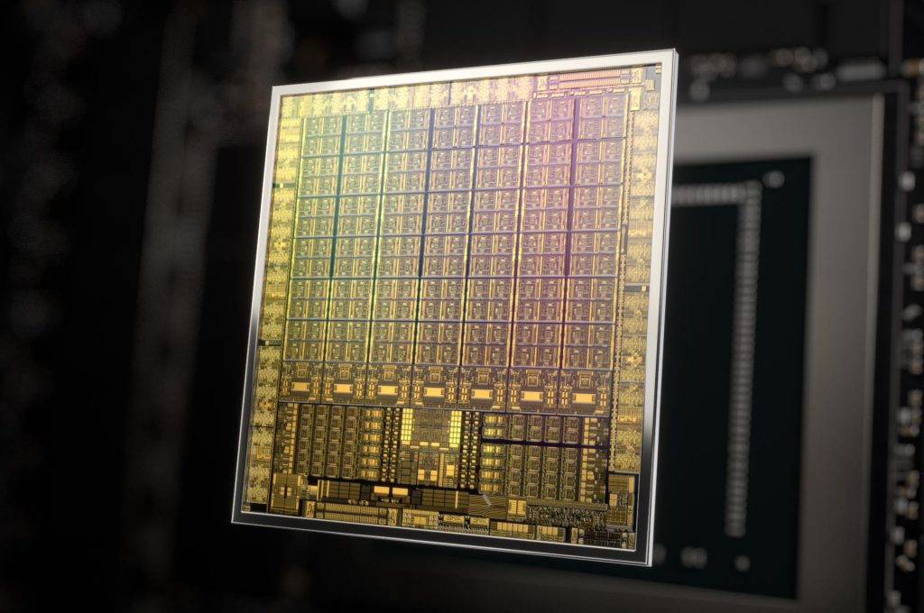
The more powerful of the two 8nm Ampere chips intended for gaming and graphics applications is called GA102 and is used in the RTX 3090 and RTX 3080 cards. Physically, it contains seven basic GPC (Graphic Processing Cluster) construction blocks, each of which contains 6 TPC (Texture Processing Cluster) blocks, where each TPC ise then further divided into two SM blocks of 128 shaders. The entire GA102 has 84 SMs and thus 10,752 shaders. In each SM block there is one RT core (for a total of 84) and four tensor cores (a total of 336).
The chip is 628.4 mm² in size and consists of 28.3 billion transistors, there’s 6MB L2 cache (and a number of 128KB L1 caches are distributed in individual blocks, these are also improved compared to Turing). In addition to SM blocks that contain compute (and also texturing) units, the chip also integrates other blocks like multimedia engine and GDDR6X memory controllers that optionally support GDDR6 with a total bus width of 384 bits.
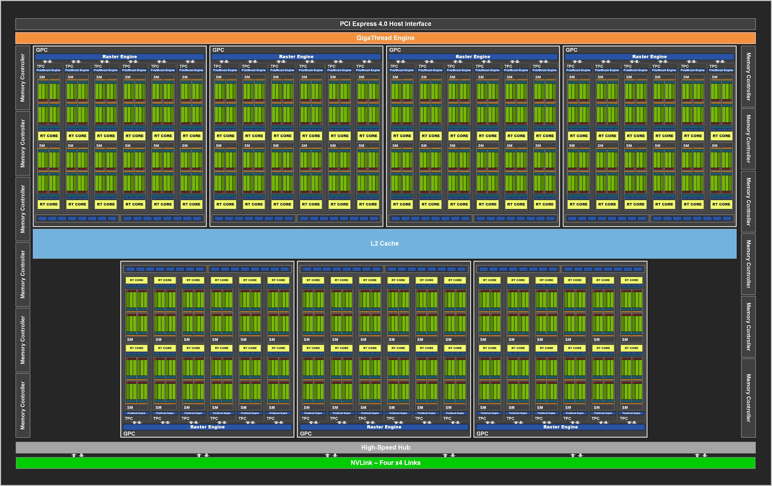
The GA102 also offers third-generation NVLink interface for connecting two GPUs (configurations with three or four cards are not supported). It consists of a total of four ×4 interfaces, which give a total throughput of up to 56.25 GB/s in both directions.
The GA102 is used in a partically disabled configuration in both currently announced GeForce SKUs. GeForce RTX 3090 uses an in almost full power config, with only two SM blocks being disabled, so the card loses 256 shaders, 8 tensor cores and 2 RT cores. The GeForce RTX 3080 is cut more significantly, losing one entire GPC and four more SMs – leaving it with only 8704 shaders (68 SM blocks), 68 RT cores and 272 tensor cores. The memory bus is reduced to only 320 bits, i.e. 2 of the 12 channels are switched off.
GA104
Besides GA102, Nvidia is redying a cheaper Ampere GPU, which should contain 48 SM blocks (6144 shaders), 192 tensor cores and 48 RT cores. This chip is used in GeForce RTX 3070, but again with some cutting down: only 46 SM/5888 shaders and 46 RT cores/184 tensor cores are left active. The organization of the chip is different – it has six GPCs, in which instead of 6 TPCs just 4 TPC blocks are present. Each TPC then has two SM blocks (from this level the rest is the same as in GA102).
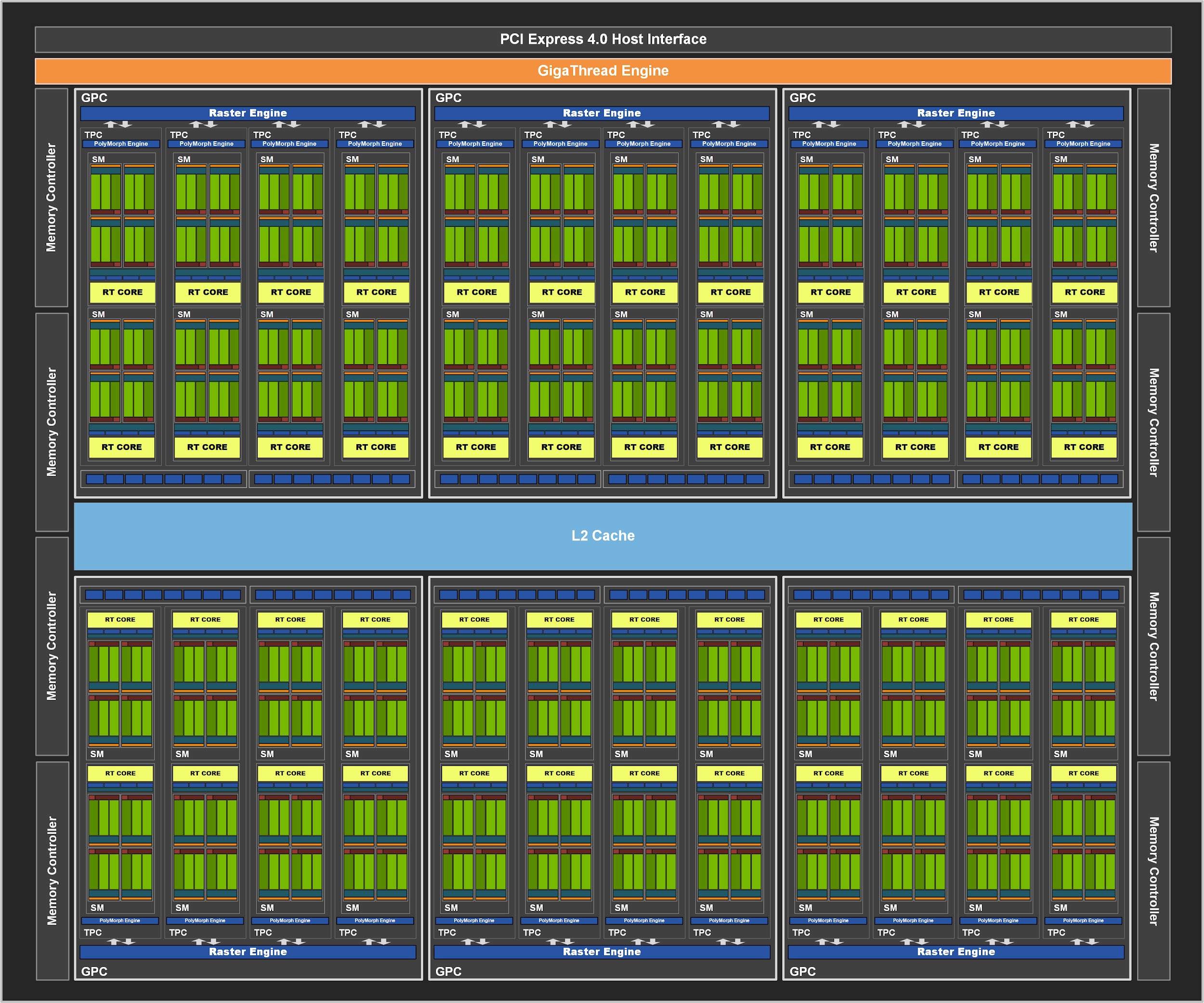
This chip has a 256-bit memory controller which is so far only paired with GDDR6, but it is possible that GDDR6X is also supported. The chip uses 4MB L2 cache and, according to Nvidia, consists of 17.4 billion transistors. Its die size is 392 mm².
ROPs will now be tied to GPC blocks
A relatively important change happened in the organization of ROP units of Ampere GPUs. Previous architectures had them tied to a memory controller and L2 cache, so for example a 192-bit card always had to have 48 ROPs, a 256-bit one 64 ROPs, 384-bit would have 96 etc.
In Ampere, Nvidia removed this dependency and ROPs are instead tied to GPC blocks and scale with their count. Each GPC block should have 16 ROPs, so the GA104 chip contains 96 ROPs and the GA102 chip increases it to up to 112 ROPs thanks to seven active GPC blocks (RTX 3080 is limited to 96 ROPs because just 6 GPS are active).
In terms of hardware, September was a green month with the release of the new generation of Nvidia GPUs, GeForce RTX 3000. They are based on the new Ampere architecture. In this article we are going to discuss what’s new compared to Turing: the new SM architecture doubling the number of shaders, the manufacturing process and the characteristics of the two chips that have been unveiled so far.
New SM block and shader architecture
Probably the most important change happened in shaders at the level of SM blocks and is related to the fact that Ampere now advertises 128 instead of 64 shaders (“Cuda cores”) per SM block and the total number of units/Cuda cores has more than doubled. It doesn’t however mean that a single SM in Ampere has twice as much resources and performance, it’s a little more complicated.
In fact, this architecture is a follow-up on the change that Nvidia has already made in the Turing and Volta GPU architectures. Originally, with Maxwell and Pascal, there were 64 shaders in one SM block and these supported FP32 (floating point operations, which are most important in the GPU) and INT32 (integer) instructions. In reality, the structure is such that the SM block contains four subsections each connected to its own warp scheduler and load/store units, and each warp scheduler sends operations to 16 FP32/shader units in form of one single 16-wide SIMD vector (a “warp”). All 16 units compute the same operation (warp) at a time, just operating on different data value. One SM is in other words akin to four 16-wide SIMD units (this is why it’s inaccurate to talk about 64 “Cuda cores”).
Processing two FP32 operations in parallel
In the Volta and Turing architectures, Nvidia has made a big change and added separate INT32 units capable of doing integer-only operations in parallel to FP32 units. Instead of one 16-wide operation (warp) in one cycle, the subsection/warp scheduler in Turing can send two warps to be executed – one FP32 warp to the main units, and if there also is and integer instruction (warp) ready, it sends it to a separate INT32 SIMD unit. In total, the SM block can now process 64 FP32 operations in one cycle as Pascal can, but in addition 64 INT32 operations can be handled in parallel with them. Integer instructions are less common (the ratio to FP ops fluctuates, but say 3:1 on average), but sending them to a parallel unit frees up the FP32 unit for more operations and greatly increases performance per 1 MHz.

And it turns out that the doubling of shaders in Ampere is, in fact, just another modification of this arrangement. Nvidia retained the ability of the SM block (or subsection) to process two operations in one cycle. But this time, there’s not a FP32 unit and INT32 unit connected in parallel, but a FP32 unit and a second unit that can do either INT32 or FP32 operations. Ampere can thus perform two floating point operations per cycle instead of one (which is 2× faster compared to Turing/Volta), or one FP32 and INT32 as Turing/Volta could. However the FP32 + FP32 combination is a more likely to happen in code, so now both of these pipelines (or data paths) will be used most of the time, while in Turing the INT32 pipeline was used perhaps only a half or third of the time.
With this, Ampere significantly increases performance per 1 MHz, but it doesn’t double the performance of Turing. Other bottlenecks can also slow down the computations, but the main reason is that only the FP32 + FP32 scenario has seen 2× performance boost, while in the case when FP32 + INT32 scenario, the performance is the same as for Turing.

Number of shaders in the specifications
Physically, one SM block is still actually made up of four subsections with a warp scheduler sending warps to 16-wide units, but now two of these 16-wide vectors/warps can be executed simultaneously. For Turing, Nvidia has not counted the units for INT32 operations as separate shaders, so those GPUs did not advertise a double number of shaders in their specifications. But since in Ampere this second unit can also execute FP32 instructions, Nvidia now has a reason to count it as a separate shader, and thus now one SM block officially counts as 128 shaders and a GPU with a given number of SMs now has twice as many shaders as it would have with the Turing architecture.
For example, TU104 and GA104 apparently both have 48 SMs, but for Turing this counts as 3072 shaders while for Ampere as 6144 shaders. This has the side effect that performance per one shader probably is higher for Turing GPUs compared to Ampere, although this is hardly important. The overall performance of the GPU or the performance per SM block (that has increased) is what matters.
By the way: this architectural change only applies to the gaming version of the Ampere architecture. Interestingly, the computing Ampere for servers (GA100 chip, Nvidia A100 card) does not use this, its shaders are arranged in the same way as in the Volta architecture, and the total number of shaders is therefore only 64 per SM block for GA100.
New 3rd generation Tensor core
This is not the only change in the SM block. Nvidia has also updated the architecture of Tensor cores used for neural network-based artificial intelligence computations (employed by DLSS) as well as RT cores used for ray tracing.
Tensor cores are reused from the computational version of Ampere and their main new feature is the use of the Structured Sparsity technique, where the core skips calculations upon zero values in the vector during matrix operations (the algorithm itself can round down values close to zero). Other values are then shifted to the spots freed up by ignoring these zeros, thus freeing up the tensor core to do more actual calculations.
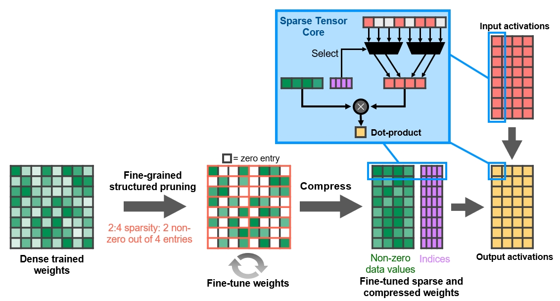
As a result, a given computation is performed with only about half the number of total FMA ops, so the tensor unit now effectively gives the performance equivalent of twice its actual TFLOPS, when Structured Sparsity is used.
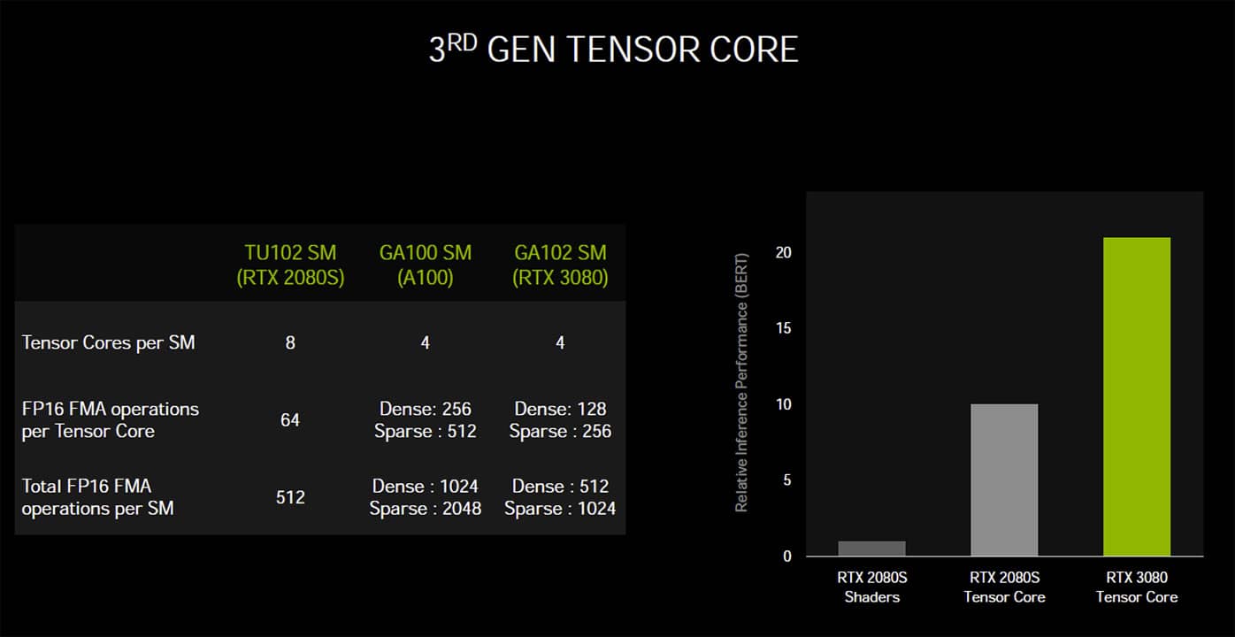
There are 4 tensor cores per SM block in the gaming Ampere, each providing 128 FP16 FMA operations per cycle. In Turing, there were eight cores were capable of 64 operations per cycle, so that would boil down to the same unchanged performance. But with the use of the aforementioned Structured Sparsity function, Ampere can offer twice the performance. Based on this, Nvidia states that the performance in artificial intelligence is doubled (or even higher, because Ampere has more SM blocks).
2nd gen RT core
The units used for ray tracing are only present in the second generation in Ampere, not in the GA100 compute chip. Their architecture and operation is probably similar to how they worked in TUring – they still search for ray intersections with bounding volume boxes of the BVH hierarchy and then for intersections with triangles that make up objects of the scene, as defined by the DXR standard within DirectX 12 Ultimate.
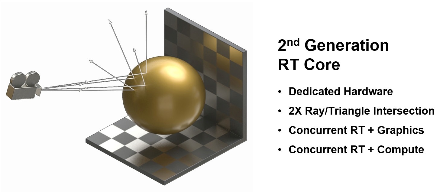
However, according to Nvidia, the compute throughput of these cores, which they have to perform these operations, is significantly higher, up to twice as much. Another improvement is that RT cores can now work simultaneously with tensor cores, which was not allowed at Turing, where only one or the other was allowed to be active at a time.
RT cores can do hardware acceleration of motion blur effect
In addition to this performance improvement, the RT core in Ampere supports another new feature. Nvidia has built in the ability to apply a motion blur effect into its architecture. This can be done when computing the intersection of the beam and the object. The intersection is temporally averaged with the intersections for the previous moments in time, and through this the resulting image is blurred as if the motion blur effect was applied separately.
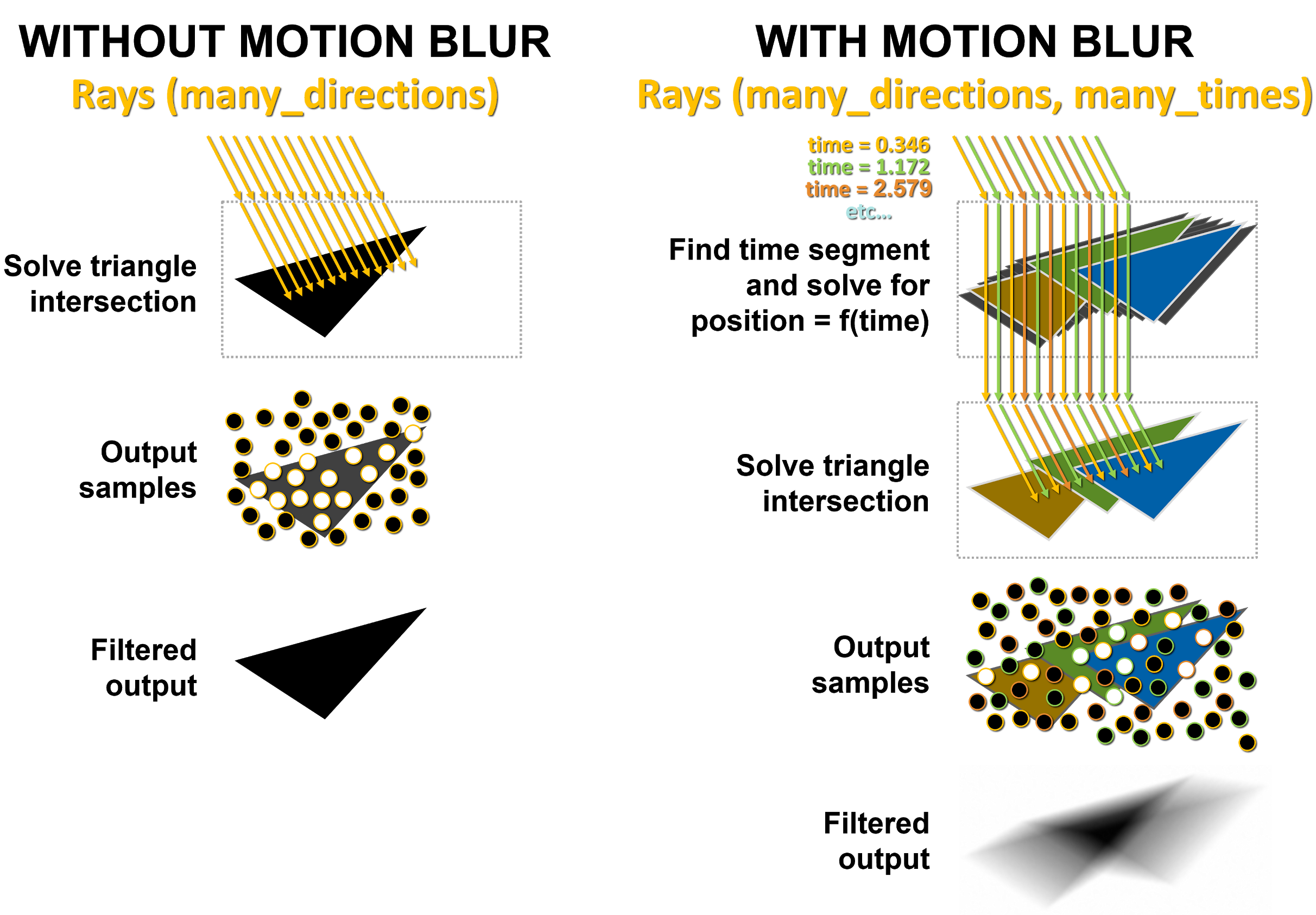
This hardware-accelerated motion blur will naturaly only be possible when ray tracing rendering or ray tracing effect is used in the game, it won’t be usablet when the game is rendered by classic rasterization.
In terms of hardware, September was a green month with the release of the new generation of Nvidia GPUs, GeForce RTX 3000. They are based on the new Ampere architecture. In this article we are going to discuss what’s new compared to Turing: the new SM architecture doubling the number of shaders, the manufacturing process and the characteristics of the two chips that have been unveiled so far.
PCI Express 4.0 and RTX IO
The Ampere GPUs are the first from Nvidia to use PCI Express 4.0 (or almost – Nvidia released the GeForce MX450 for laptops a few weeks ago, which has a Turing TU117 chip in a new revision, which surprisingly supports PCI Express 4.0 ×4). PCI Express 4.0 delivers twice as much bandwidth to the graphics card when communicating with the system, with one line transferring 2 GB/s instead of 1 GB/s with PCI Express 3.0. Loading textures or other data is twice as fast with PCIe 4.0.
Ampere is not yet fast enough to be significantly limited by PCI Express 3.0 bandwidth. According to techPowerUp’s testing, you will mostly lose just about 1% of performance in games if you insert the card into a PCIe 3.0 ×16 slot instead of PCIe 4.0 ×16. This becomes a bit bigger concern if you only give the card eight PCIe 3.0 lines, but the drop will still be just a few percents.
PCIe 4.0 bandwidth is to be exploited for new mode of direct reading of compressed textures from NVMe SSD, using DMA transfer which avoids without going through the CPU and RAM. This technique is called DirectStorage, Nvidia calls it RTX IO.
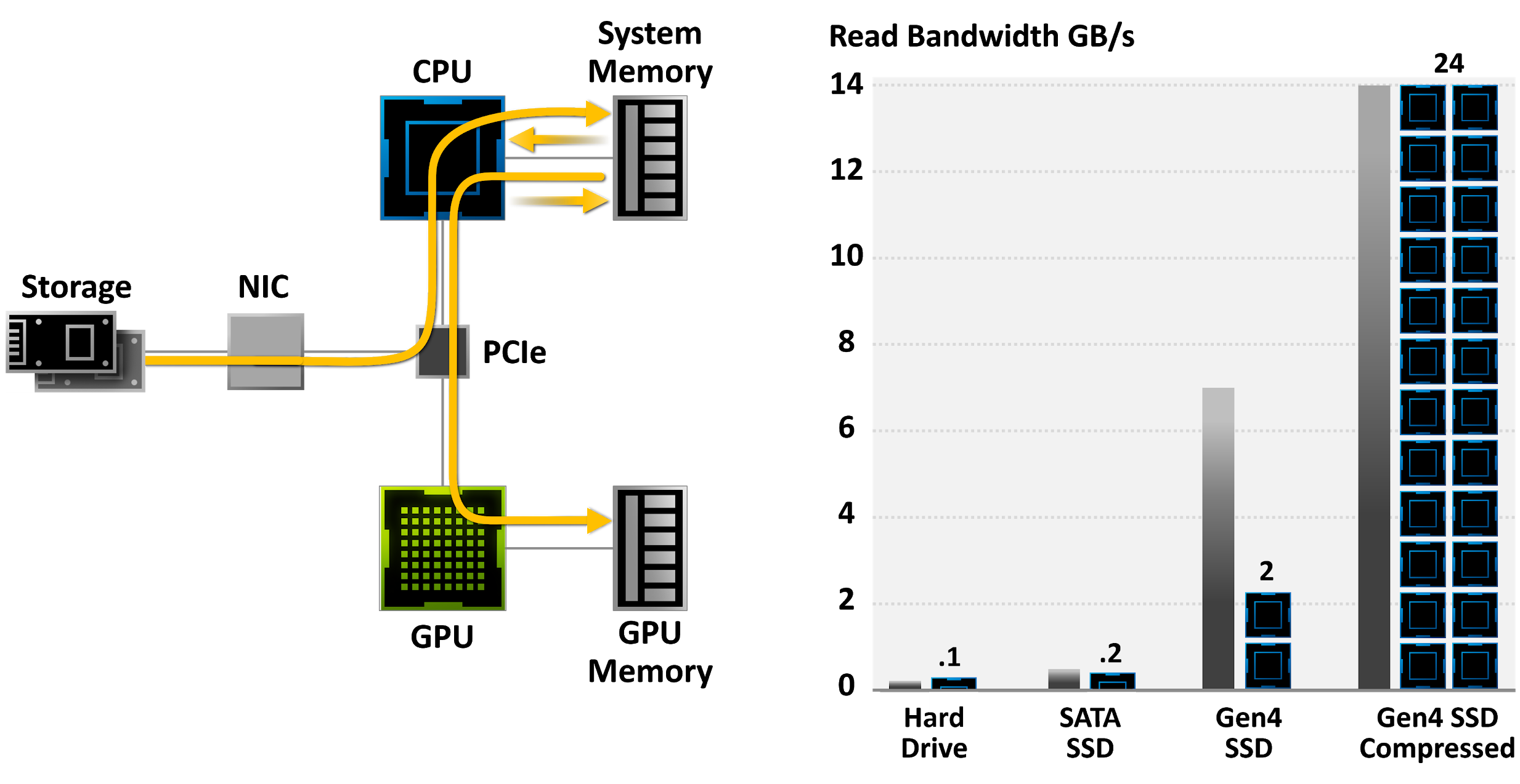
With this technology, textures are decompressed directly on the GPU using shaders, which, according to Nvidia, allows to extract a significantly larger amount of data, that would otherwise take up many cores if this was performed on CPU. For example, the GPU freed up to 24 CPU cores in the demo demonstrated during Ampere’s announcement event, but this might be a bit of an corner case. The RTX IO/DirectStorage implementation is not a fully hardware feature by the way. The decompression runs on general-purpose compute units (shaders). Thanks to this, Nvidia is going to add this capability to the Turing generation graphic cards with a driver update.
HDMI 2.1 and 8K support
The Ampere GPUs are the first standalone graphics cards to support HDMI 2.1 output, with a maximum bandwith of 48 Gb/s. As a result, connected TVs will be ale to handle resolutions of up to 8K at 60 frames per second or 4K at 240 frames per second. This also includes HDR picture.
However note that this is not an uncompressed full quality. These resolutions will require the use of lossy DSC 1.2a compression and also the conversion to subsampled YUC 4:2:0 colorspace (where the brightness component has a resolution of 8K, but the color/chrominance places only have 4K resolution).

There are no changes for DisplayPort output, here Nvidia only supports DP 1.4a. It is probably still too early for DisplayPort 2.0 to appear. The graphics cards can use HDCP 2.3 copy protection on both DisplayPort and HDMI.
Support of video in AV1 format
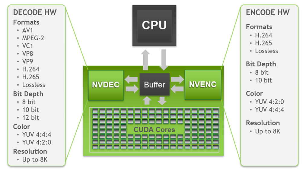
In addition to 8K display driving, the Ampere GPU can also work with video of this resolution (8K is 7680 × 4320 pixels). Ampere has a new decoding block that supports, in addition to the classic H.264 and H.265 (HEVC) and VP9 formats also the new AV1 format. This novelty is also introduced by Intel’s Tiger Lake and it looks like it will also be supported in the Radeon RX 6000.
The GPU should be able to play back AV1 video in profile 0 and level 6.0, which means in 8 and 10 bit color depth, but only with 4:2:0 color sampling, not with 4:2:2 or 4:4:4 coding (4:4:4 is supported for HEVC). 8K playback at 60 frames per second is supposed to be supported.

On the other hand, video compression (encoding) into AV1 is not yet possible. Ampere only contains new video decoders, not encoders. The NVENC hardware encoder was more or less taken over from the previous generation of Turing and supports compression of up to HEVC and VP9. However, Intel doesn’t have an AV1 encoder yet either. It makes sense to add just playback support at first, which takes less work.
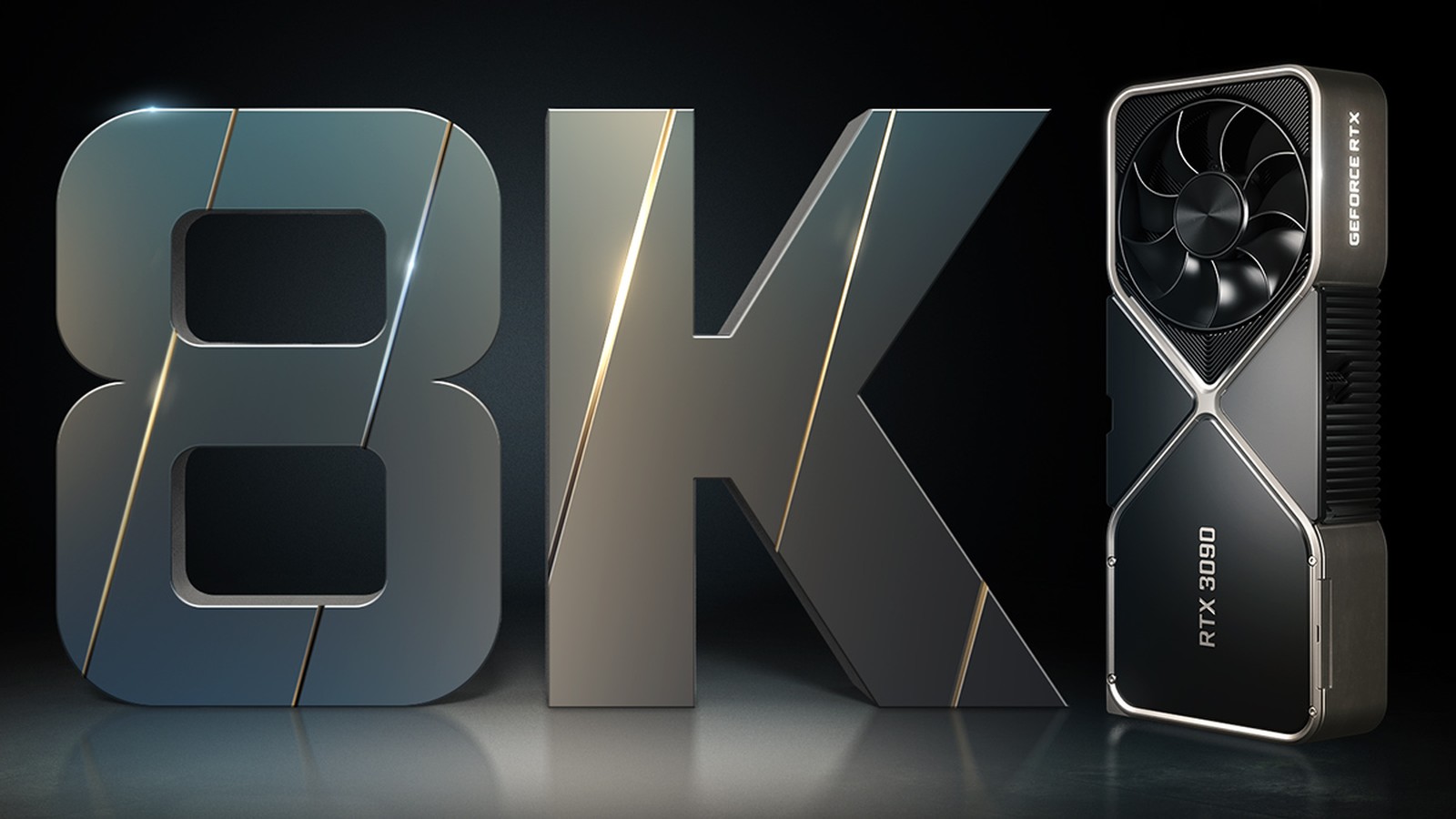
8K gaming (using DLSS)
Especially with the GeForce RTX 3090 (but it should be similarly possible with the RTX 3080, which isn’t too far behind in performance) Nvidia also announced that thanks to Ampere, it is now a possibility to game in the resolution of 8K/7680 × 4320 pixels, which has 4 times more pixels than 4K. However, this does not mean native rendering in 8K, Nvidia is only playing about upscaling a lower resolution rendering to 8K display resolution.
Nvidia uses its DLSS upscaling for this, which now supports 8K output in the new version (DLSS 2.1). This uses the newly added Ultra Performance mode, which has even higher speed and lower quality than the previously fastest “Performance” mode. The original Performance setting performs upscaling with a magnification factor of 2× in both dimensions, so for 4K output, the image is actually rendered on the GPU only at resolution of 1920 × 1080 pixels and then upscaled to 3840 × 2160 pixels using tensor cores.
DLSS with 8K resolution (Ultra Performance) works with an even larger upscaling factor of 3× in both dimensions. This means that when gaming in 8K, the graphics actually only renders image at the resolution of just 2560 × 1440 pixels, all the rest is upscaling. This probably means stronger blurring and artifacts. Thanks to such a low native resolution, the games should clearly achieve quite playable FPS, but of course, the image quality will be far from native 8K rendering.
New architecture, but building upon the innovations of Turing and Volta
So that’s it for the Ampere GPU architecture. In general, we can perhaps say that it is not as an innovative jump as Turing and Volta were, in which RT cores and tensor cores first appeared (the Volta GPU had tensor cores before Turing, but only for servers). Ampere is more about increasing the performance of these new units. An exception to this, however, is the doubling of the number of shaders, which was very well kept secret and provided a big surprise at the launch. Even this feature, however, is kind of finishing a work that was already a been started in the Turing and Volta architectures. But Ampere significantly improves it.
What happens is that Ampere will in all its aspects (shaders, memory, RT cores, tensor cores) probably reach significantly higher performance, so the novelties from the previous generation will now be better useble in games. And also, there will be more games with ray tracing effects now compared to years 2018/2019.

Nvidia has done a good job on this architecture. There’s probably just a single flaw, that being the high performance is accompanied by an increase in power consumption, whether this is the fault of the 8nm process, or whether Nvidia simply decided to tap this source to make the cards faster. A significant part of the performance boost the RTX 3000 cards bring to the table is thus achieved by increasing power consumption, while efficiency has not increased as much, at least in RTX 3080 and RTX 3090 (RTX 3070 is more efficient). However, this may be temporary, it is possible that in the next evolution fo Ampere made on 7nm or 5nm process, Nvidia will return to lower power consumption and higher efficiency.
Performance of the individual GeForce RTX 3000 cards is something that we’ll leave for actual reviews.
English translation and edit by Lukáš Terényi