GA102 and GA104 chips specifications, the first two Ampere units
In terms of hardware, September was a green month with the release of the new generation of Nvidia GPUs, GeForce RTX 3000. They are based on the new Ampere architecture. In this article we are going to discuss what’s new compared to Turing: the new SM architecture doubling the number of shaders, the manufacturing process and the characteristics of the two chips that have been unveiled so far.
Ampere GPUs: GA102
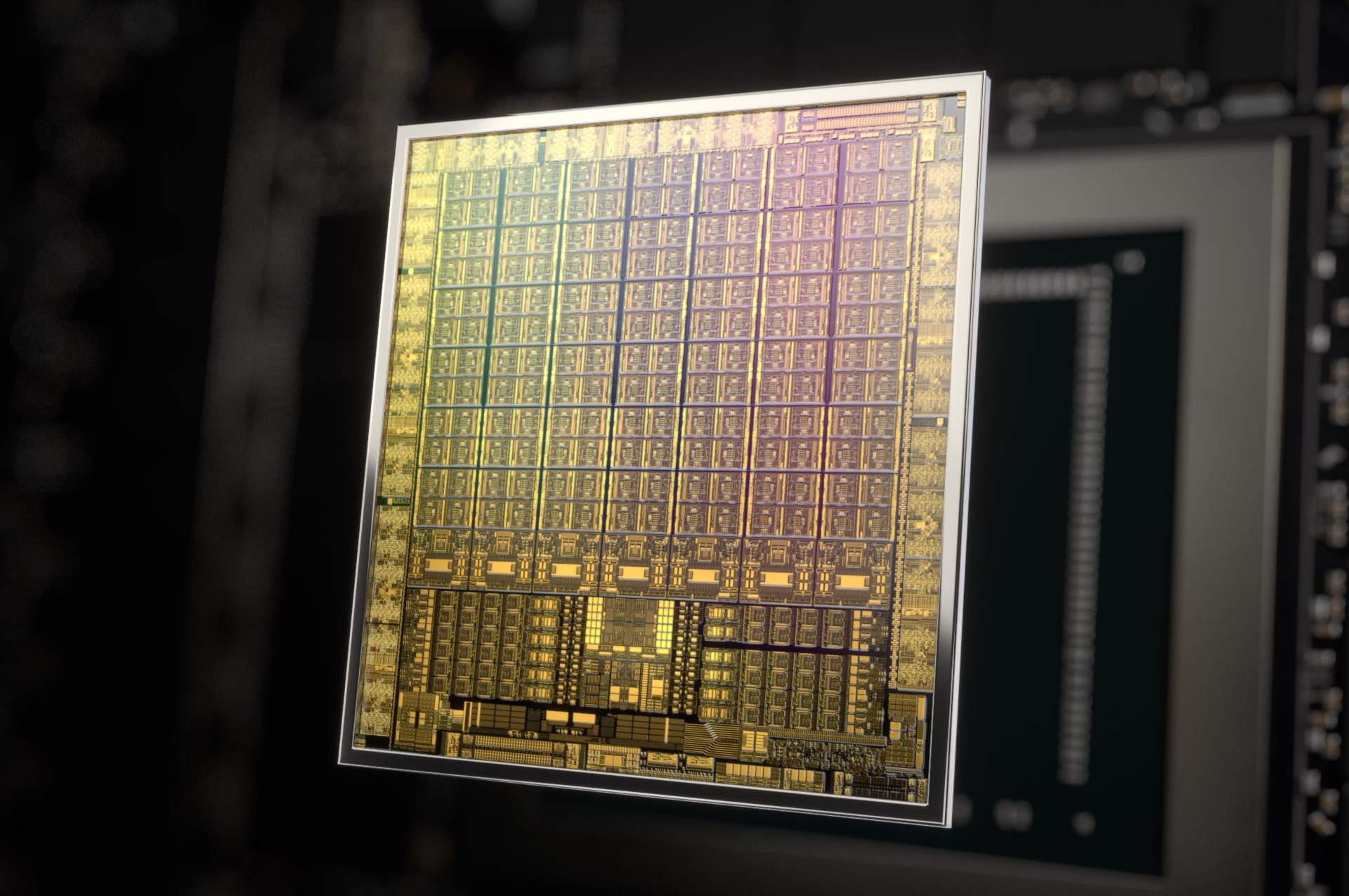
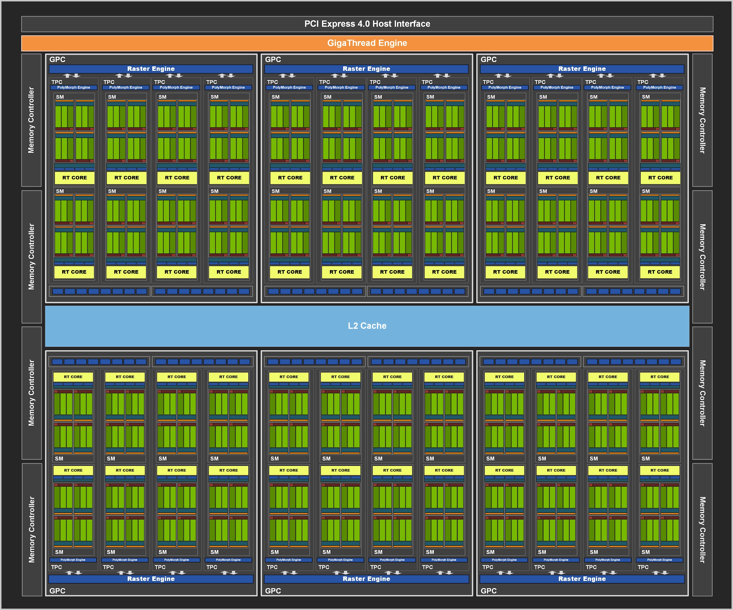
The more powerful of the two 8nm Ampere chips intended for gaming and graphics applications is called GA102 and is used in the RTX 3090 and RTX 3080 cards. Physically, it contains seven basic GPC (Graphic Processing Cluster) construction blocks, each of which contains 6 TPC (Texture Processing Cluster) blocks, where each TPC ise then further divided into two SM blocks of 128 shaders. The entire GA102 has 84 SMs and thus 10,752 shaders. In each SM block there is one RT core (for a total of 84) and four tensor cores (a total of 336).
The chip is 628.4 mm² in size and consists of 28.3 billion transistors, there’s 6MB L2 cache (and a number of 128KB L1 caches are distributed in individual blocks, these are also improved compared to Turing). In addition to SM blocks that contain compute (and also texturing) units, the chip also integrates other blocks like multimedia engine and GDDR6X memory controllers that optionally support GDDR6 with a total bus width of 384 bits.

The GA102 also offers third-generation NVLink interface for connecting two GPUs (configurations with three or four cards are not supported). It consists of a total of four ×4 interfaces, which give a total throughput of up to 56.25 GB/s in both directions.
The GA102 is used in a partically disabled configuration in both currently announced GeForce SKUs. GeForce RTX 3090 uses an in almost full power config, with only two SM blocks being disabled, so the card loses 256 shaders, 8 tensor cores and 2 RT cores. The GeForce RTX 3080 is cut more significantly, losing one entire GPC and four more SMs – leaving it with only 8704 shaders (68 SM blocks), 68 RT cores and 272 tensor cores. The memory bus is reduced to only 320 bits, i.e. 2 of the 12 channels are switched off.
GA104
Besides GA102, Nvidia is redying a cheaper Ampere GPU, which should contain 48 SM blocks (6144 shaders), 192 tensor cores and 48 RT cores. This chip is used in GeForce RTX 3070, but again with some cutting down: only 46 SM/5888 shaders and 46 RT cores/184 tensor cores are left active. The organization of the chip is different – it has six GPCs, in which instead of 6 TPCs just 4 TPC blocks are present. Each TPC then has two SM blocks (from this level the rest is the same as in GA102).
This chip has a 256-bit memory controller which is so far only paired with GDDR6, but it is possible that GDDR6X is also supported. The chip uses 4MB L2 cache and, according to Nvidia, consists of 17.4 billion transistors. Its die size is 392 mm².
ROPs will now be tied to GPC blocks
A relatively important change happened in the organization of ROP units of Ampere GPUs. Previous architectures had them tied to a memory controller and L2 cache, so for example a 192-bit card always had to have 48 ROPs, a 256-bit one 64 ROPs, 384-bit would have 96 etc.
In Ampere, Nvidia removed this dependency and ROPs are instead tied to GPC blocks and scale with their count. Each GPC block should have 16 ROPs, so the GA104 chip contains 96 ROPs and the GA102 chip increases it to up to 112 ROPs thanks to seven active GPC blocks (RTX 3080 is limited to 96 ROPs because just 6 GPS are active).
- Contents
- New manufacturing process 8N: Samsung technology enhanced especially for Nvidia
- GA102 and GA104 chips specifications, the first two Ampere units
- New shader architecture, how is it with 2× FP32 units
- PCI Express 4.0, HDMI 2.1, AV1, 8K video and 8K (upscaled) gaming