


Zen 5-based AMD processors will launch this year (perhaps in Q3). Unlike Zen 4 which was just Zen 3 refined, Zen 5 will be another big upgrade, and according to various hints including statements by the architect Mike Clark, it could be AMD’s most interesting core since the first Zen. Interestingly, up until now, the only information about it has come from a single YouTuber source. But it has just been officially confirmed directly by AMD.
All of the specific information about the nature of Zen 5 cores (aside from the info that desktop CPUs will use 4nm chiplets) comes from one leak by youtuber Moore’s Law Is Dead. He revealed both a schematic of the core, but as you’ll recall, also projections of the performance increase per 1MHz of clock speed the core is supposed to provide. The so-called IPC is supposed to improve by 10–15+% according to these slides (the plus is probably supposed to mean that the 10–15% range is a conservative lower bound).
While we will keep on being in the dark on performance for a while, AMD has now pushed a patch adding support for optimizing for Zen 5 processors to the GCC compiler, used mainly for building open source software. The patch is interesting to us because it describes a number of aspects of the core and corroborates the slides published by Moore’s Law is Dead a while ago. This means their authenticity has likely been proved, and we can now rely on them with a fair degree of confidence.
Tip: Leaked AMD documents show Zen 5 and 6 IPC and architecture details
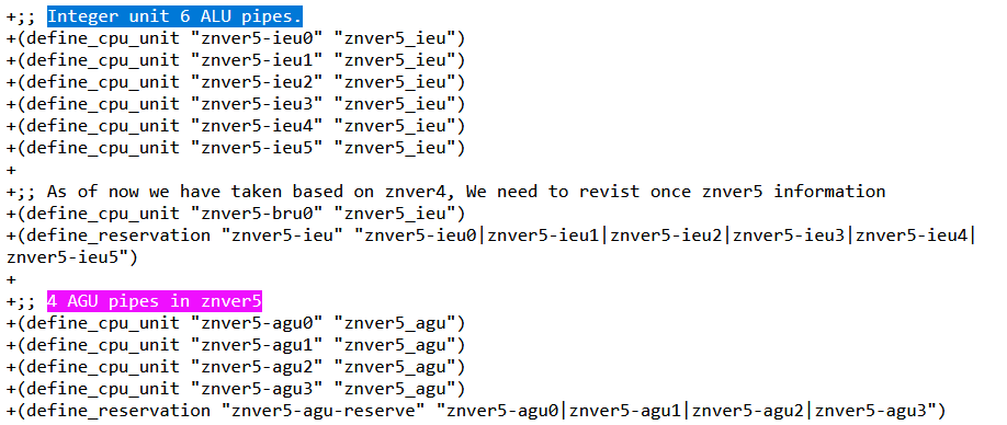
Widened core: ALUs and AGUs added
Patches for GCC confirm the widening of Zen 5 microarchitecture. From the first to the fourth generation, these cores have maintained a very similar basic structure with four arithmetic logic units (ALUs) that execute the brunt of most common instructions, although there are three AGUs (that perform memory write and read ops) in Zen 3–4 but only two in Zen 1–2. This contrasts with the higher number of execution units in Intel P-Cores, not to mention some ARM cores. The Cortex-X4 ALU, for example, already contains eight ALUs.
It was interesting that AMD was able to extract relatively higher performance from this particular number of exeucution unts than its competitors, but Zen 5 finally goes further in this parameter. The patch confirms that the core has six ALUs and four AGUs. This could facilitate a significant increase in IPC, though initially the utilization of these extra units may not be as high and further advances in IPC may only be garnered gradually in subsequent generations, much like how Zen 2, 3 and 4 were able to gradually get more and more performance out of the four ALUs already present in Zen 1.
It is not yet clear whether the load/store pipelines (AGUs) have been increased in width from 256 bits to 512 bits to be able to read and write a 512-bit wide vector for AVX-512 instructions in one cycle.
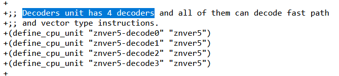
On the other hand, there is one area where the core has not in fact been widened. The number of instruction decoders remains at four. However, x86 processors, including Zen architectures, use the so-called uOP cache as an alternative solution, which stores already decoded instructions. Most of the time, the processor should take instructions from the uOP cache, which can deliver significantly more instructions per cycle than the four decoders and this path is also more power efficient on x86 CPUs. Thus, the number of decoders is not as important for Zen 5 as in ARM processors without a uOP cache.
Tip: ARM unveils record-breaking Cortex-X4 core with eight ALUs
Native 512-bit wide AVX-512 execution
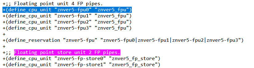
The FPU unit (which crucially also handles all SIMD instructions including integer SIMD) does not seem to have extra pipelines added compared to Zen 3 and 4, there will be four pipelines used for different operations in the FPU again. However, GCC confirms that Zen 5 contains 512-bit SIMD units for the first time in AMD processor history. These units will supports processing most AVX-512 instructions in a single cycle, whereas Zen 4 has 256-bit units like the Zen 2 and Zen 3 cores (which could only do 256-bit AVX2) before it. Therefore, the previous core executed 512-bit AVX-512 instructions in two passes, each calculating half the width of the vector. This SIMD expansion in Zen 5 seems to correspond to the addition of a second port for Floating-point store operations. However, the FP store units are apparently still 256-bit wide, so 512-bit operations are performed by combining the two units.
The widening of the SIMD unit width to 512 bits alone means that the theoretical compute performance given in FLOPS (but the same applies to ops working on integer data types) is doubled. This should allow Zen 5 to catch up with the raw performance of Intel’s cores in all parameters, so using AVX-512 should now give AMD an advantage in servers, whereas until now it gave Intel a chance to catch up with the higher general performance of Epyc processors (Intel might still have an advantage in the AMX matrix instructions, which are different from AVX-512).
However, the patches for GCC show that further improvements have been made. The SIMD units now have the ability to handle shuffle (permute) operations with three pipelines instead of two, so that three such operations can be performed per cycle instead of two. There appears to have been a redistribution of some operations between ports in the FPU. Floating-point addition has had its latency reduced from three to two cycles, which should directly improve performance as successive ops where one instruction uses the output of the previous one for its output can be executed sooner.
The integer part also has some improvements of this kind. It looks like the two newly added ALUs can do more than just the simplest operations, or AMD has beefed up the existing ALUs. While the previous cores could only process CMOV and SETCC in two of the three ALUs, Zen 5 can process these instructions in four of its six ALUs, up to four of these ops per cycle, according to the GCC patch.
There is also information in the patch that division and square root calculations should faster, these instructions have their latency reduced by one or more cycles for most data types.
Zen 5 will be able to do some AVX-512 instructions that Intel lost (or abandoned?)
The patch also shows that the Zen 5 core will also to support some AVX-512 instructions that Zen 4 does not support yet. This ISA extension has a rather large (and criticized) number of subsets. Zen 4 supports a significant portion thereof, but not the MOVDIRI, MOVDIR64B, PREFETCHI, and AVXVNNI instructions – the latter will be useful for AI, but it is actually just a 256-bit version of the VNNI instruction that was added by Intel for E-Cores, whereas Zen 4 can do it in its original 512-bit version. AVXVNNI will be useful mainly for compatibility with big.LITTLE Intel processors. Zen 5 adds all these instructions.
In addition to these, Zen 5 also supports an extension called AVX512VP2INTERSECT (AVX-512 Vector Pair Intersection to a Pair of Mask Registers), which is a curious obscure subset. These instructions were added to Intel’s Tiger Lake processors (Willow Cove architecture), but then Intel apparently changed its mind or found some problems in the implementation, because subsequent architectures, including the current Intel Sapphire Rapids server processors, no longer support AVX512VP2INTERSECT.
It is possible that the AVX512VP2INTERSECT will make a comeback in Intel architecture. Intel still bases everything in its portfolio that is newer than Tiger Lake on one architecture, the Golden Cove core, so it’s possible that AVX512VP2INTERSECT is broken only in that one microarchitecture, or even just in its server version that is used in Sapphire Rapids and Emerald Rapids. Interestingly, the Alder Lake and Raptor Lake client CPUs seem to have supported this instruction for a while, until Intel forcefully disabled their AVX-512 support. However, the recently presented plans to reorganize 512-bit instructions under the AVX10 umbrella also do not mention this extension, so it is possible that its return is not planned anymore.
Recommended reading: Intel replaces AVX-512 with AVX10. Now also for big.LITTLE processors
This might create a funny situation where AMD supports something that Intel does not, somewhat similarly to the case of FMA4 instructions. This doesn’t have to be to the benefit of Zen 5 though, it can become a liability too. After all, the support for this instruction will consume transistors that Intel will be able to spare, while software developers may stay away from using it because of the lack of support on Intel CPUs. This is a disadvantage that smaller competitors often have to deal with.
However, it’s not the case that Zen 5 overaly supports more AVX-512 instructions than Intel cores. It should have more coverage than Intel’s desktop and laptop processors (Ice Lake, Rocket Lake, Tiger Lake), but the Sapphire Rapids and the new Emerald Rapids server processors have a few extra instructions that Zen 5 won’t be able to execute yet.
Sources: GCC / AMD, AnandTech Forum (1, 2)
English translation and edit by Jozef Dudáš
⠀

I hope they’ll push saner power limits and heat density this time, zen4 heats up way too much ESPECIALLY when using a single core and it’s much harder to cap properly than just setting PPT (as clocks alone don’t determine heat output, it’s about the actual load profile too, but oh well, setting it to -500 don’t hurt too much to be honest)
but at the end of the day I’d love to see mobos that aren’t built like a tank just to not burn when you put a CPU out of the box in them
ZEN5 on 4nm is not a good idea. It will be overheating and AVX512 is obsolete, AVX10 will replace it. I recommend to wait for ZEN6 on 3/2nm with AVX10.