

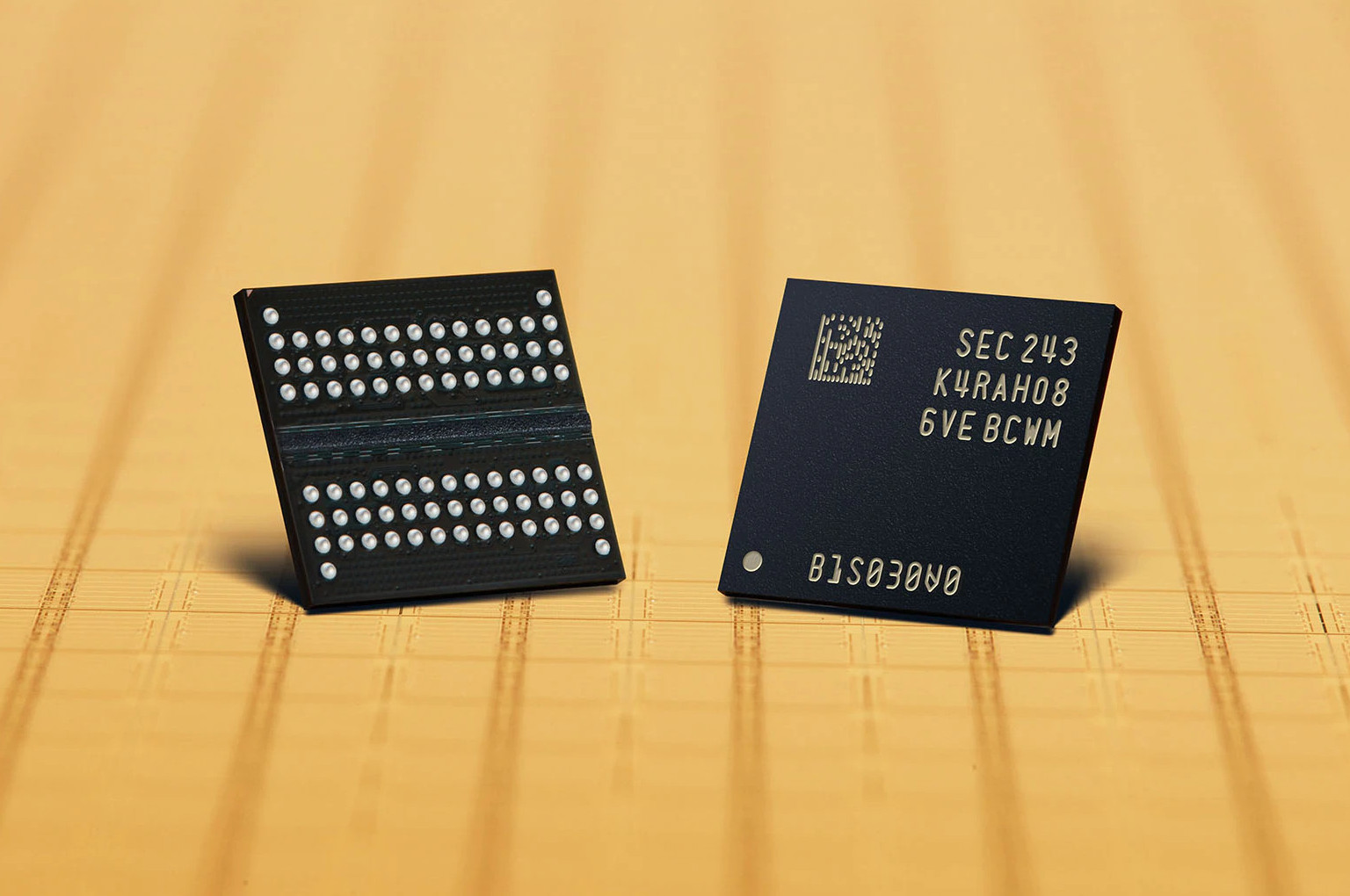
DRAM used in operating memory has long been experiencing problems. It doesn’t have the best scaling to new manufacturing nodes, which limits capacity growth. Things used to be similar with 15nm NAND Flash, the last gen before planar technology was replaced by 3D NAND. That literally breathed new life (or at least TBWs) into SSDs. However, a stacked “3D” version is now shaping up for DRAM as well, giving hopes it could be similarly groundbreaking.
Vertical Channel Transistor
Samsung has now unveiled a roadmap for the development of its DRAM technology (on which all different types of DRAM – from HBMx to GDDRx and DDRx to LPDDRx – should be based). And according to the roadmap, sometime between 2026 and 2028, the company should change the DRAM cell structure to a partially 3D one – presumably by deploying 3D FinFET transistors in the DRAM cell. This technology is called Vertical Channel Transistor (VCT).
Apparently, this should make it possible to shrink the cell by move some of the elements that are currently placed next to each other in a plane to be placed underneath each other. This means that it will be possible to allocate a larger area for the structure with the capacitors of the cells holding their values. These are a part critical for scaling DRAM to smaller manufacturing nodes, as they are the most “resistant” to die shrinking and thus increasing chip capacity. This is because the smaller the capacitor, the harder it is to maintain the stored value, preventing the architects from shrinking them significantly with every new process node.
If the cell layout manages to save on other circuit components, a larger percentage of space is left for capacitors and memory density is increased without degrading capacitor performance.
Stacked 3D DRAM?
This should then be further improved by the next generation of DRAM, which will be stacked like NAND, and thus can be truly described as 3D DRAM. Apparently, it would rotate the cell structure so that the now vertically stacked capacitors would form horizontal “sticks” in the chip structure, stacked in multiple layers. Address and data wires would then run across them, and transistors would also be in “stacks”.
This should allow DRAM capacity to scale further without the cell having to physically shrink further. Instead, capacity increases will come from increasing the number of layers in the chip, which has worked very well with 3D NAND the last decade or so. Actually, before the advent of 3D NAND, shrinking planar NAND cells had reached a point where 15nm chips already had very little reliability and lifetime. Hopefully, the stacked architecture will be at least a little bit as successful in DRAM and allow further increases in RAM capacity without increasing prices.
But the arrival of this technology is more distant. Samsung reckons it could be deployed sometime in the early years of the next decade (2030–2031?). But there is probably still a lot of development to do and the path to this technology is far from clear, so it would not be strange at all if it faced delays and was only be put into practice later.
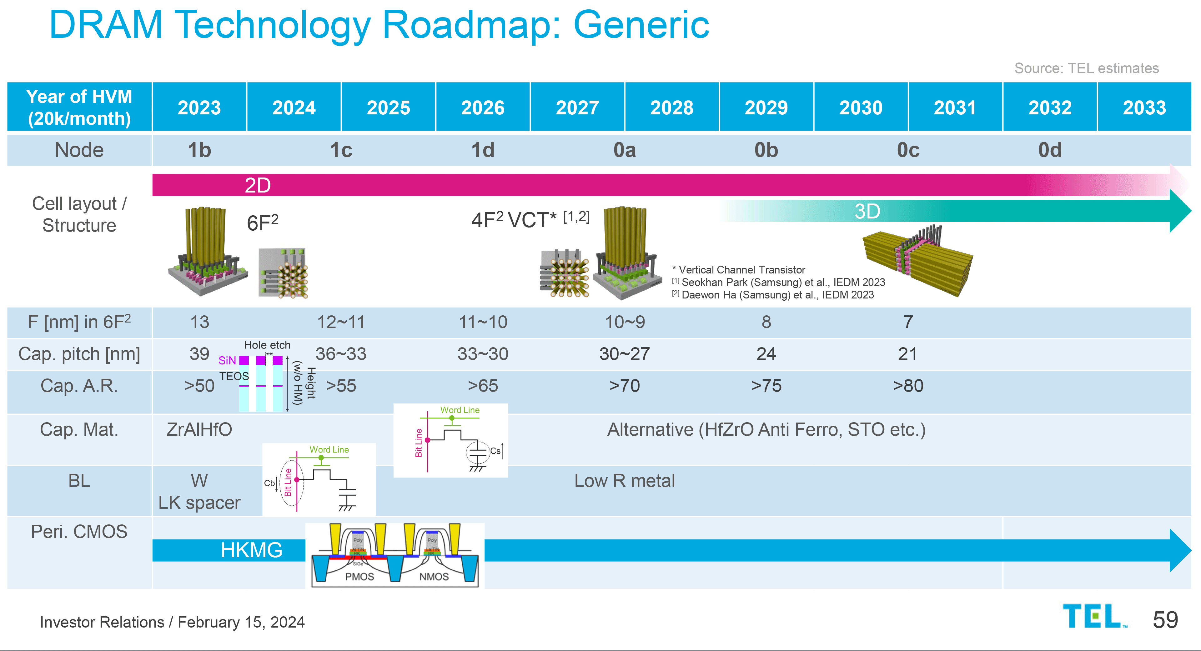
Samsung states that they will require new materials for building the capacitors in the cell and for the address and data wires (bitlines) even for the first step of vertical channel transistor (VCT) memory. There has long been a demand for some similar transformative improvements to DRAM architecture, such as the revolutionary 3D NAND for flash memory, bit all this long time we didn’t see it happen, suggesting that the transition to 3D DRAM will certainly not be an easy task.
But the fact that it is now at least officially included in the plans of one of the largest memory manufacturers (Samsung was the first to introduce 3D NAND, too) gives hope that a change in operating memory is in the works, even if it is still a long way off. Other DRAM manufacturers are likely to develop similar 3D architectures after or alongside Samsung.
We mentioned that the transition to stacked DRAM should be key to further increasing RAM (and perhaps also GPUvideo memory) capacities. But it will be similarly crucial for maintainting future pace of performance and power efficiency improvements, future DRAM will need to keep scaling in those departments as well.
Will 3D DRAM help against RowHammer?
But there could be one more positive besides that. The shrinking of cells in planar DRAMs has led, among other things, to their greater susceptibility to the RowHammer attack, which compromises security by allowing malicious code to reach memory contents in a single line that it should not be able to access by manipulating adjacent lines because DRAM is susceptible to “flipping” adjacent cells. This is a pretty insidious problem, and it probably gets progressively worse as cells get smaller. Perhaps switching to stacked DRAM could stop the cell shrinking and thus alleviate the RowHammer problem, similar to how 3D NAND put a stop to the process of gradual deterioration of NAND write endurance that plagued the planer NAND as it was moving to smaller and smaller process nodes.
However, this is just our speculation or wishful thinking, it’s not exactly certain. The problem that interference from adjacent cells can change (corrupt) the memory content in DRAM will probably not go away completely. It is also possible that the properties of the stacked structure itself will create a similar weakness.
Sources: SemiEngineering, Tom’s Hardware
English translation and edit by Jozef Dudáš
⠀