


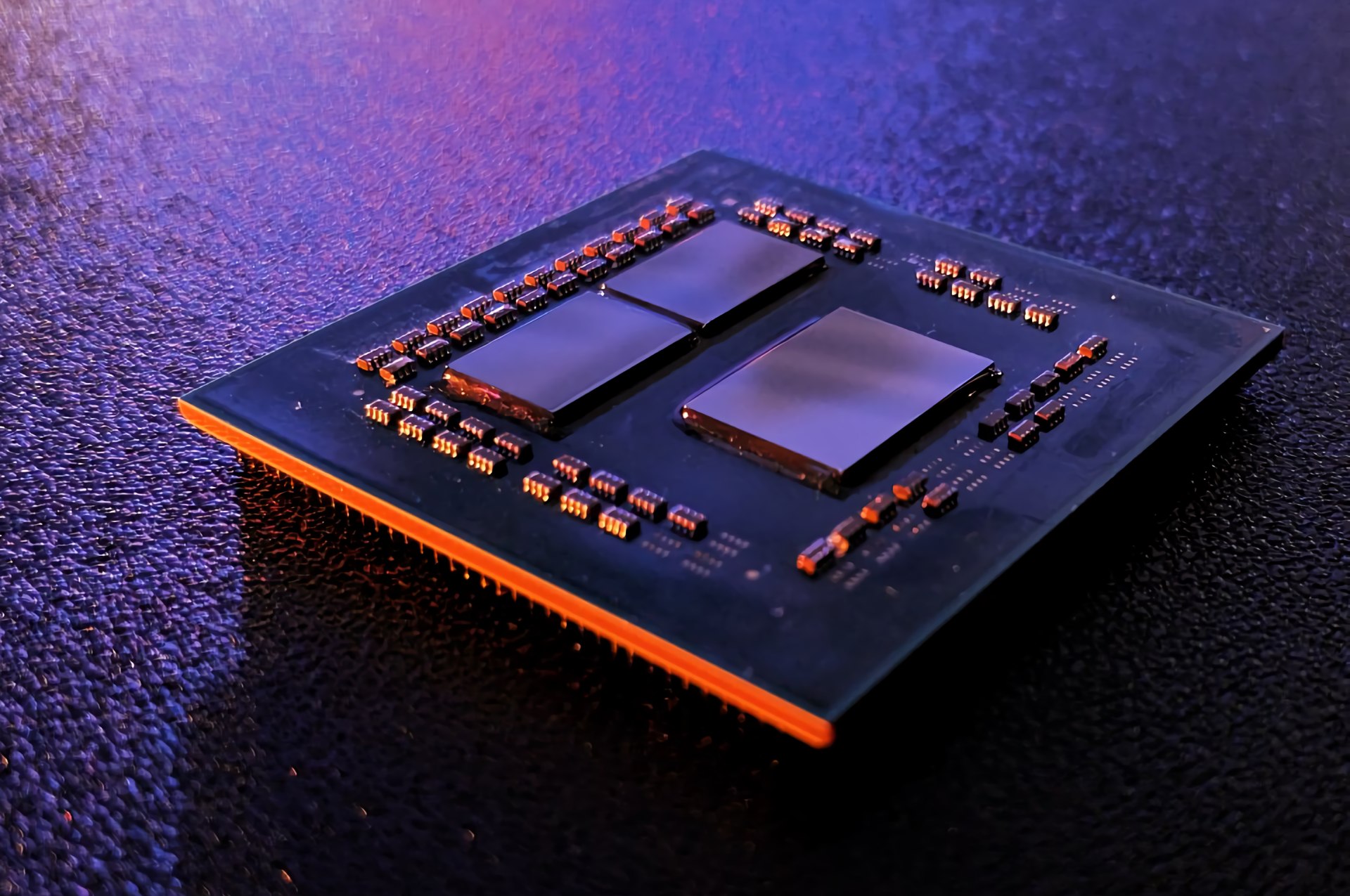
After Intel’s hybrid CPUs, AMD is preparing its own big.LITTLE scheme that uses a mix of Zen 4 cores and a new Zen 4c variant that will be used in servers but also in laptops. However Zen4c is and at the same time is not a little core. While having much smaller footprint, it is said to be fully architecturally equivalent to the large core, including (almost?) the same performance per 1 MHz. The only little thing about it is clock speed.
AMD presented bits about the little(?) Zen 4c core during Computex and at the same time an analysis of this architecture appeared on the SemiAnalysis website. So far, it seems to mainly be because these cores will form the codename “Bergamo” Epyc cloud processors (hence the C in Zen 4c), but tiny-style zen cores should eventually appear in mobile APUs as well – maybe already in this generation in the “Phoenix 2” chip, which is supposed to complement the eight-core Phoenix APUs with cheaper models.
Much smaller core with the same IPC and features
If the concept of Zen 4c were to be summarized: According to AMD’s CTO Mark Papermaster, the purpose of this core is to significantly increase the transistor density (and thus reduce its area) so that more of them can be crammed into a given area specifically for the needs of these cloud processors. The core area is almost halved compared to the classic large Zen 4. However, unlike E-Core or the usual little cores from ARM, these cores keep “identical functionality” to Zen 4.
According to AMD, the Zen 4c core (its codename is reportedly Dionysus) is not cut down in virtually anything compared to Zen 4 and should have the same IPC (performance per 1 MHz). What is also crucial is that AMD has confirmed full compatibility at the instruction set level, so Zen 4c will also support AVX-512 instructions and this will not be an issue like it was with Intel’s big.LITTLE take.
Tip: AVX-512 on Ryzen 7000s: how useful is it and is AMD’s implementation better than Intel’s?
In Zen 4c, the organization of cores and caches was changed, but only the L3 cache was reduced in capacity. The Zen 4c core still has 32KB of L1 cache for data and 32KB of L1 cache for instructions, also the L2 cache remained at 1MB (which is perhaps a surprise, but this is probably due to the goal of preserving IPC and also to optimize for cloud instances for which private cache is important).
Reduction occurred only in the L3 cache. AMD cut it to 16 MB for one CCX block with eight cores. By contrast, the L3 in the desktop and server Zen 4 is 32 MB. But AMD has been reducing the L3 cache on mobile APUs/SoCs for a while now, so the 16MB L3 cache of the Zen 4c basically just matches what the Zen 4 mobile cores have. This might be one area where the claim that the IPC will not decrease will not be entirely valid – some applications may feel the impact of a smaller L3 cache.
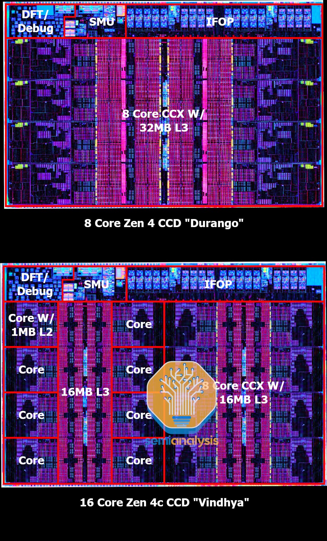
Zen 4c will use CPU Compute Die with 16 cores (their codename is Vindhya) in servers, and the cores will be placed in two CCX blocks, no longer just in a single one per die. Each block should have 16MB of L3 cache, so the total L3 cache per CPU Compute Die will remain the same. This may be why the L3 cache per one CCX had to be halved in the first place. The L3 cache in Zen 4 takes up half of the CPU Compute Die area so 2×32MB would balloon the die size.
Density increased thanks to physical design targetting lower clock speeds
The main difference from Zen 4 is that AMD has redesigned the physical implementation of the architecture and used libraries aimed at higher transistor density instead of libraries designed for high performance. Also, the provisioning for TSV (vertical wiring vias for connecting 3D V-Cache) has been eliminated, which also saved space on the chip. Overall, a CPU chiplet with 16 Zen 4c cores and 2×16MB L3 cache should still measure only 72.7 mm², while the area of a regular Zen 4 is 66.3 mm². So the silicon area has increased by less than 10% when doubling the number of cores (and the amount of L2 cache).
According to the available images of the core, it seems that AMD has also changed the layout and placement of parts of the core on the chip. Apparently, the blocks are less partitioned and synthesis could “stuff” them closer together. This is probably because delineated partitions isolating individual blocks are meant to make it easier to test and verify CPU functionality on a new architecture, with Zen 4c as a reimplementation of one already existing being less sensitive to this. Zen 4c has only four such “partitions” (frontend, execution units, L2 cache and FPU/SIMD unit). This alone saves some space that was left unused in Zen 4, because the synthesis of the circuits couldn’t overlap the partitions in before.

At the same time, standard block libraries that optimise for higher density and design that sacrifices the ability to achieve high clock speeds (which go well above 5 GHz for desktop Zen 4 processors) were used. High-speed design uses extra transistors and elements (or larger transistors) and many locations to improve the achieved clock frequencies. Zen 4c eliminates this, as it only expects or aims to run at significantly lower clock speeds. The resulting circuit can then be implemented in a smaller footprint. Different parts of the core are said to have their area reduced by up to 35–45%. This is while using the same 5nm node (TSMC N5). The key to this increase is believed to be mainly the simplification of the wiring (in the metal layers) between the transistors that results from the abandonment of high-speed design.
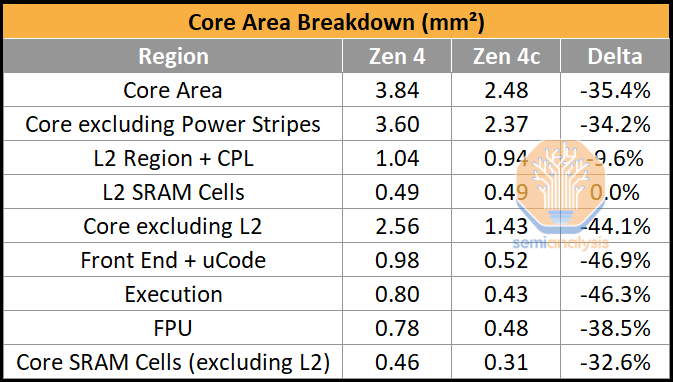
It seems that the area of the L2 cache itself is one thing that has not been shrunk– its SRAM cells still have the same density and area – but its control circuitry has been reduced in size. However, some other SRAM blocks in the core logic have been made more dense, with AMD using 6T cells (made of six transistors) instead of 8T cells with eight transistors. 8T cells were previously used because of the dual-port feature (two sets of read/write wires can be connected to them), but TSMC has developed special 6T cells with pseudo dual-port functionality that can do this through double-pumping (two accesses happen sequentially in one cycle via one single interface). And Zen4c reportedly uses this technology.
It is not yet fully confirmed whether AMD has reduced the number of pipelines in the FPU/SIMD unit, as it did with the “Zen 2 Lite” core used in the PlayStation 5, Xbox Series X and S consoles or the Mendocino APU. This would of course decrease the IPC in tasks that use these units.
Boost will decrease a lot, but the base and all-core clock speeds in a server CPU can be almost the same
The specifications of two Epyc “Bergamo” processors with this architecture are already known. The full-fat model is called Epyc 9754 and contains 128 cores (256 threads) in eight CPU dies. The processor uses the same IO die as the common Epyc 9004 “Genoa” CPUs, but according to some indications, eight CPU dies is probably the maximum for it, whereas 12 (which would allow models with 192 cores) is probably not doable with the current substrate and package design.
The clock speeds of the Epyc 9754 are only 2.25 GHz base and 3.1 GHz in boost. Particularly the boost of the compact Zen 4c cores is much lower according to this (the regular Epyc 9654 has a boost of 3.7 GHz), but the base clock speeds didn’t suffer as much (it’s only a 150 MHz lower compared to the regular model), so it seems that this lower clock range is no longer a problem for the Zen 4c design that has given up higher clock speeds. TDP of this SKU is 360 W.

In addition to this model, there is a lower cost Epyc 9734 processor that has one core disabled in each CCX, leaving it with 112 cores and 224 threads. Its clock speeds are further dialled down to 2.20 GHz base and 3.0 GHz in boost. This model has a TDP of 340 W. Both processors support 12-channel DDR5-4800 memory (by which we mean 64-bit channels, but with DDR5 they are actually always made up of two 32-bit channels – in short the memory has a width of 768 bits, if we don’t count ECC, which is also supported). The socket used is the same SP5 socket as with Epyc 9004 “Genoa”, both CPUs should be compatible at platform level. Existing servers and motherboards probably just need a firmware update to get compatibility with Bergamo.
Low clock speed core can be useful in MT tasks
The specifications of these server processors may already hint at the ways the Zen 4c core or its successors could be useful in PC processors. At first glance, only reaching clock speeds of, say, 3 GHz instead of the 5+ GHz of the desktop Zen 4 sounds bad. However, this maximum clock speed is mostly important for single-threaded applications. Especially in laptops, however, the CPU clock speed is significantly reduced in just about any multi-threaded workloads and can reach levels that can already be handled by this scaled-down Zen 4c core, let’s say something around 3 GHz. So, if in such a situation additional Zen 4c cores are involved alongside the classic Zen 4 cores, there shouldn’t be any problem as long as their IPC is really the same – the performance characteristics from the code’s point of view remain the same and the software doesn’t have to deal with the differences between P-Cores and E-Cores like in the Intel case. You just need to ensure that the operating system uses these cores only in multi-threaded workloads and prefers the larger cores with higher clock speeds when scheduling low-threaded programs and games.
Thus, a hybrid (big.LITTLE) processor could be created, that would have a group of Zen 4 cores, which will be able to run at high clock speeds in single-threaded applications and in games (games would need a higher number of these cores, likely 6-8 at least). The other Zen 4c cores group’s time to get to work (and shine?) would come in multi-threaded applications, where due to the limited TDP the clock speeds would always going to be low anyway, and both the Zen 4 and the Zen 4c cores would basically end up at roughly the same clock speed, maybe somewhere around those 3 GHz. The ideal result would be if the Zen 4c cores were able to run at that clock speed with lower power draw than the big Zen 4 (if not, the benefit would only be in lower silicon costs for the manufacturer).
Zen 4c in a low-end Ryzen 7000?
According to some indications, this principle will possible be tested for the first time in the low-cost “Phoenix 2” processor. Needless to say, it would be on a smaller scale. Apparently this SoC has only two large Zen 4 cores (so they will mainly be useful for single-threaded applications and may not be sufficient for advanced games), plus four little Zen 4c cores. Note that it is possible that the Zen 4c designation will not be used for these client processors, as the name is tied to the server role (C is for cloud).
Further reading: Paradigm shift in AMD processors. First big.LITTLE Ryzen will be the Phoenix 2 APU
Even these inexpensive processors should however show what clock speeds can realistically be achieved by Zen 4c and consequently how suitable it is for laptops and whether it could possibly be used in a desktop at all. Desktop usage will face the most obstacles, as the highest-performance Ryzen 7000 SKUs run around 5 GHz even in all-core boosts (they do pay for it with very high power draw in multi-threaded workloads, with up to 230 W PPT limit) and Zen 4c may not be able to get close to that.
Sources: Tom’s Hardware, SemiAnalysis
English translation and edit by Jozef Dudáš
⠀
