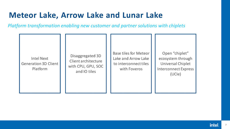
After the Raptor Lake processors due this year, Intel is preparing an ambitious new generation codenamed Meteor Lake for 2023. These chiplet-based processors and will be the first to use the 4nm process. However, it turns out that Intel is only making one of the four chiplets. The company that has always taken pride in its own factories will rely on its main competitor for most of the silicon in the Meteor Lake processor.
We already knew that some parts on Meteor Lake will be manufactured by TSMC (for example, GPUs) from various leaks. But now, ahead of this year’s Hot Chips conference, Intel has revealed a schematic of the Meteor Lake processor and revealed which processes are used in its (four or five total, depending on how you count) chiplets. And it turns out that, from a manufacturing process perspective, there’s more “outsourced” about Meteor Lake than in-house.
There is only one tile from Intel
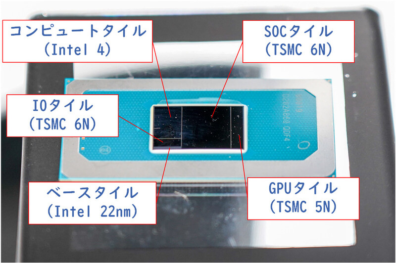
Meteor Lake is made up of four active chiplets (or as Intel says, tiles). Intel puts the main emphasis on the Compute Tile containing the CPU cores – both big (P-Core) and little (E-Core) – and the L3 Cache. This chiplet is 4nm, manufactured using the the Intel 4 process. Saying that this part, albeit smaller in size, is the most important is probably justified, because the implementation of CPU cores is usually the most difficult and complex task.
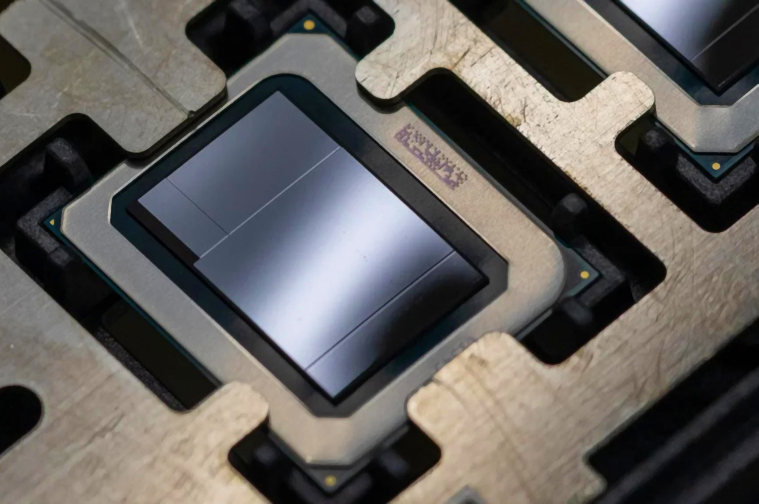
On the other hand, this chiplet is the only one of the active parts of Meteor Lake that will be manufactured with Intel technology, which is noteworthy. In the following photo from the Japanese website PCWatch, you can see the position of this chiplet in the top left. So it’s not even a somewhat dominant percentage of the total silicon area. The photo shows a mobile version of Meteor Lake with only two large cores (it’s a 2+8 configuration, Meteor Lake-U).
In the presentation, Intel also showed a schematic of the more powerful version with six big cores (confirming that the more powerful mobile Meteor Lake-P will have 6+8 cores), where the 4nm Compute Tile is larger but still makes up less than half the area. However, this is not uncommon in today’s processors, the cores themselves make up less than half of the chip even in AMD processors or various ARM SoCs including those made by Apple.
The smaller strip of silicon, which is next to the CPU chiplet in the remaining space on the bottom left, is the so-called IO Tile and should contain, for example, a PCI Express controller (in particular, it should be its PHY). This chiplet already uses TSMC’s process, namely its 6nm N6 process. It is an EUV process derived from the 7nm process and is used to manufacture some of AMD’s GPUs (RDNA 2 and, in the future, cheaper variants of RDNA 3).
The big surprise is that the largest piece of silicon you see in the middle, the SoC Tile, is also manufactured using the TSMC process. It probably has a similar function as the IO chiplet in AMD processors – it combines some of the blocks normally forming the processor with the functionality of the chipset and should handle most of connectivity interfaces. There should also be a PCIe Root Complex and perhaps memory controllers in this part. According to a recent leak, there could even be two extra small cores present in the SoC Tile for running background tasks and similar activities, their goal is to reduce the idle power draw of the processor and the whole computer (particularly for laptop use).
Read more: Intel Meteor Lake processors have not two, but three core sizes: LP E-Core in SoC chiplet
Even the SoC Tile uses TSMC’s N6 process. It was this silicon that Intel was expected to produce with its own process, such as Intel 7, so that Meteor Lake processors would provide more opportunities to employ its own production lines. But for some reason, TSMC’s process was selected.
It may seem illogical that there are two different chiplets manufactured at 6nm. Primarily, the reasons for heterogeneous manufacturing technologies should lie in specialization, where the most advantageous process is used for each part. But then you would probably expect that an IO Tile suitable for 6nm could be coupled with an SoC Tile. But perhaps the reason why this is not the case is purely because including both in a single rectangle would work out worse in terms of the overall stacking of the tiles together – and you can’t make the chiplet L-shaped. If that constraint wasn’t there, IO Tile and SoC Tile could probably be combined into one piece, they’re probably not that different functionally.
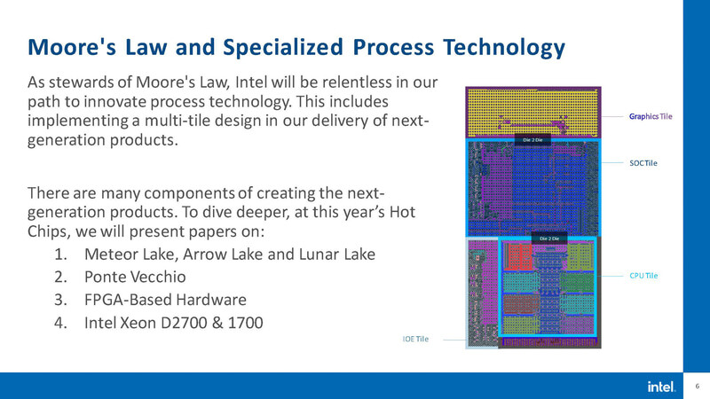
GPU Tile includes the integrated Xe LPG architecture graphics, partially derived from Xe HPG architecture used in standalone Arc graphics. Or rather, there are at least parts of it in the GPU Tile. Theoretically, for example, the video accelerators could be in the SoC Tile, and the blocks taking care of the display output are probably there as well, as this would like be optimal for power draw and battery life.
The GPU Tile is on the far right in the photo and surprisingly is quite narrow and thus low-area. It’s also manufactured at TSMC, but on the 5nm N5 process. So Intel has finally confirmed that this chiplet will not be 3nm, even though there were such rumors before. Intel could have theoretically been considering both options at the beginning and leaned towards the 5nm process due to better readiness for mass production and lower cost.
The slim GPU in the photo may be a less powerful configuration if Intel has more of them in plan. In the 6+8 Meteor Lake-P schematic shown now in Intel’s presentation, the GPU Tile looks slightly wider relative to the SoC Tile. It’s possible that this is a more powerful variant of the GPU. Meteor Lake graphics reportedly has 1024 shaders (128 EU) in the maximum configuration, so there is a room for a smaller lower-performance alternative GPU die.
Read more: Integrated GPU in 4nm Intel Meteor Lake processors will already support ray tracing
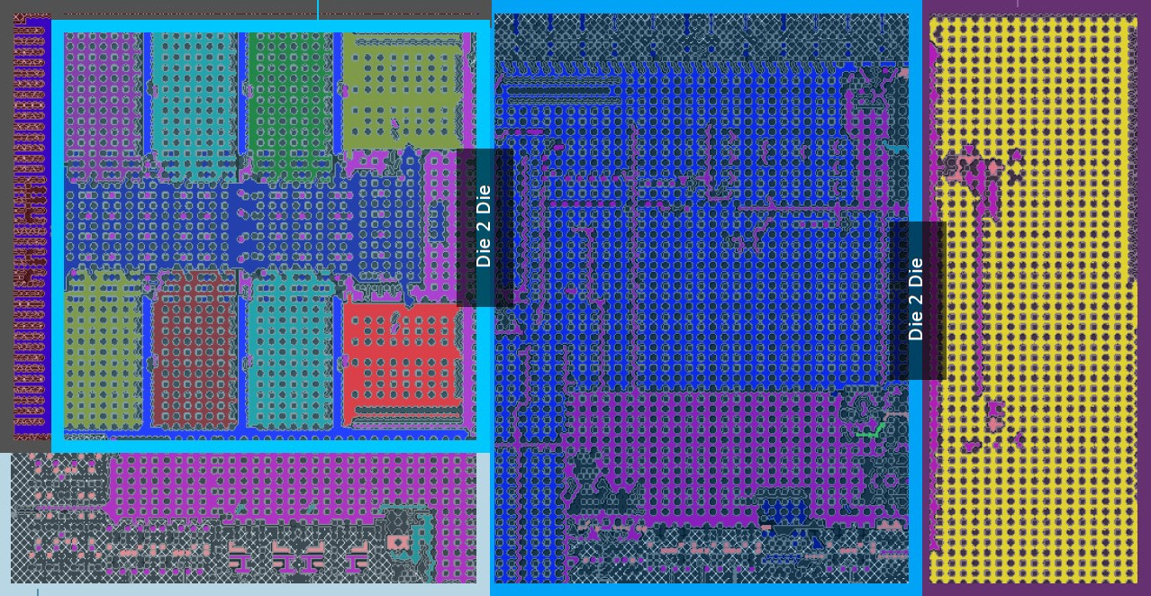
TSMC makes most of the “active” silicon – not counting the interposer
These four “tiles” are active chiplets in the sense that they contain transistors and some logic blocks. However, you could also argue that strictly speaking, TSMC does not make most of the silicon used in Meteor Lake. Why is that? Underneath these four tiles is a fifth carrier chiplet, the Base Tile, on which the upper active chiplets are stacked and connected by the advanced Foveros packaging. This Base Tile is manufactured by Intel on a 22nm process, however it is not an active chiplet, but a passive interposer, consisting only of metal layers. This interposer connects the tiles of the top layer together, similar to how interposers connect GPUs to HBM/HBM2 memories.
The question is whether this interposer forms an underlying layer in the full area of the upper tiles, or whether it is in fact just silicon bridges that occupy only a smaller area along the chiplet boundary. So in the first case, which is perhaps more likely, the area of silicon produced by Intel would technically be more than half of all the die sizes combined. However, the area of a cheap 22nm die on a mature process, made with no transistor layer and used as interposer only, does have less weight than the area of the silicon of the upper tiles that are produced on relatively advanced processes.
However, even with all these matters that arguably matter more on the reputation and symbolism levels, Meteor Lake should still be a very interesting processor (or SoC) on technological level, if just for this this complicated multi-die composition. How well it all works in practice, we should hopefully find out in the second half of next year, when these processors are expected to be released.
Sources: PCWatch, TechPowerUp, VideoCardz, Intel
English translation and edit by Jozef Dudáš
⠀