


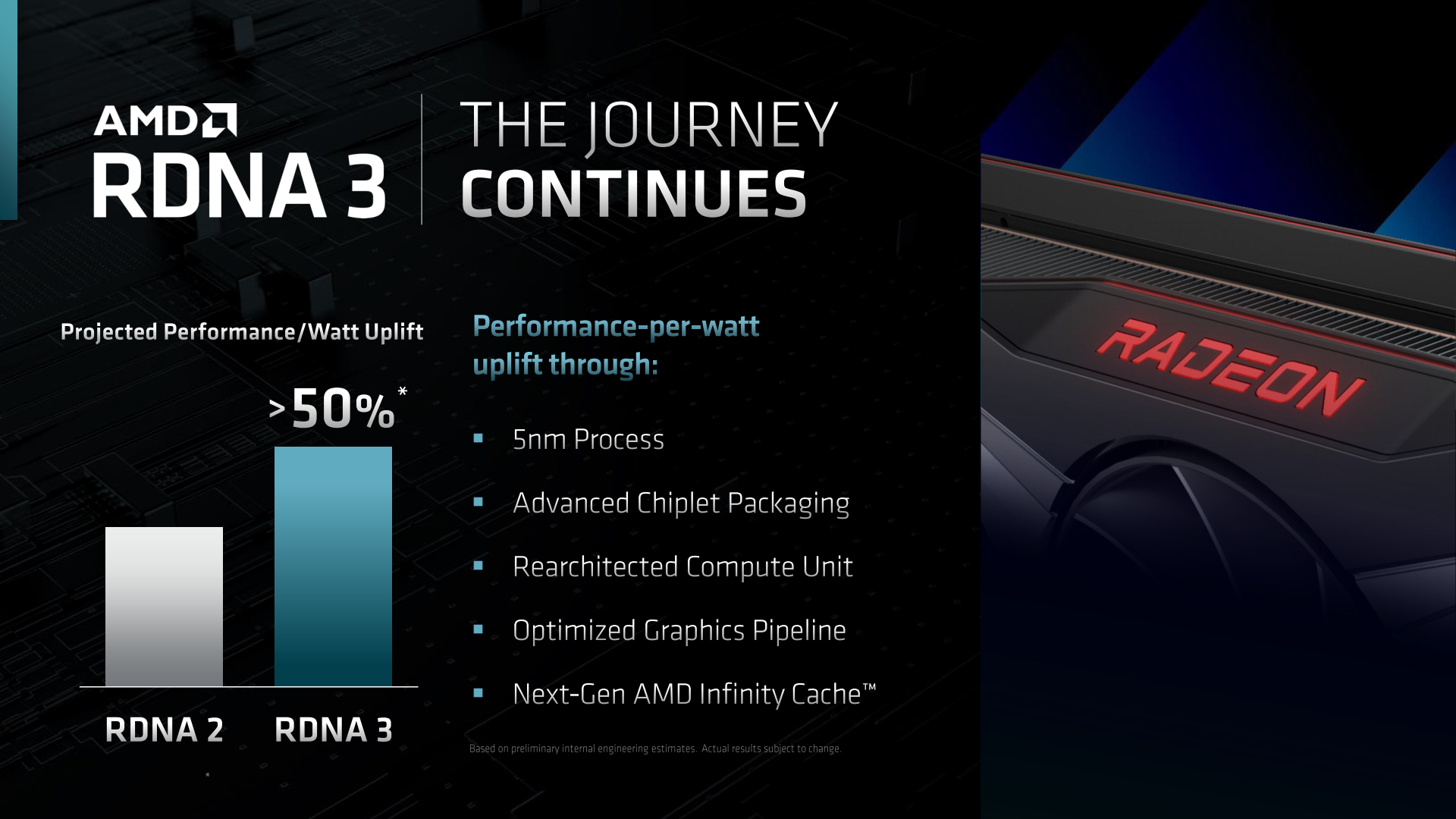
Major news has surfaced about AMD’s upcoming RDNA 3 architecture based 5nm GPUs. These chips will form the basis of Radeon RX 7000 generation graphics cards, which will compete with Nvidia’s GeForce RTX 4000 GPUs. Angstronomics has published their specifications as well as chip sizes, which raise doubts whether they can have competitive performance. On the other hand, they could be relatively low-cost.
RDNA 3 chip specs have surfaced before, in two waves – first these there was this rumor, but a few months ago we learned that the compute unit counts are lower. The Angstronomics leak is probably the most detailed (and fairly realistic looking) report yet. According to this site, AMD more or less determined the specs in 2019 and they were fixed at least some time in 2020 – this makes sense since changes can only be made long before tapeout and even longer before release. So if higher unit counts ever were considered during development (those alleged 15 360 shaders for Navi 31), it had to be before then.
Highend: Navi 31
A fairly substantial part of the previous leaks turns out to be true, but equally substantial are the things that seem to be different than previously thought. The most powerful GPU is supposed to be the Navi 31, which is now reportedly use the “Plum Bonito” cover name in the Linux drivers and internally has the gfx1100 architecture designation. This GPU will reportedly have 48 workgroup processors (WGP), which is equivalent to 96 CUs. However, a single WGP will contain twice as many shaders or FP32 units compared to RDNA 1 and 2 architectures, i.e. 256 shaders or 128 per CU. Navi 31 will have 12,288 shaders due to this (this matches the previous information given by Greymon55).
These will be divided into 6 shader engines / 12 shader arrays. What is further confirmed (at least at the level of unofficial information, it is not definitely confirmed in a strong sense of course – you still have to take this information with a grain of salt): the Navi 31 will have a 384-bit memory bus, which AMD hasn’t used for several years since the GCN architecture era. It will be fitted with GDDR6 memory, but there’s no word on what capacity or clock speed. This is not strictly speaking part of the specs of the GPU itself.
Angstronomics also confirms that the Navi 31 GPU will be chiplet-based and composed of seven chiplets, so previous leaks have not been lying about this either (unless Angstronomics is lying now). It is supposed to use a single GCD (Graphics Compute Die) chiplet that is 5nm (TSMC N5) and contains the compute units. Then attached to it are six 6nm (TSMC N6) MCDs – Memory Chiplet Dies. These chiplets will implement the memory controller part (64 bits wide) and a SRAM block that forms part of the GPU’s Infinity Cache.
Infinity Cache has been reduced
So far the rumours have hit it well, but now a change is coming. AMD will surprisingly use Infinity Cache capacities that are smaller than in the previous generation, even though they were expected to be increased. According to Angstronomics, there is only a mere 16 MB of Infinity Cache in a single MCD. Thus, the base version of the Navi 31 GPU has only 96 MB of Infinity Cache, while the currently selling Navi 21 has 128 MB of available capacity.
It’s quite the question as to what this means for achievable performance, and whether this means taht AMD will only achieve a relatively minor performance jump with Navi 31 that won’t be enough for the supposedly more than 2× generation-on-generation performance boost expected from Nvidia. In the opinion of other leakers, it seems that Navi 31 will not be able to reach the same performance as Nvidia’s most powerful chip (AD102). The latter thus seems to have secured the “crown” of the most powerful single-chip GPU, although this may come at the cost of worse power draw and price.

„1-hi“ 3D Infinity Cache
However, it is true that beyond this basic version there will also be a modification that will use special 3D modification of MCD chiplets instead of the classic ones, where two MCD chiplets are apparently connected on top of each other. This Navi 31 “1-hi” configuration will therefore have a 192 MB Infinity Cache in total.
AMD is said to have originally considered a 2-hi version, which would have apparently been three MCD chipsets on top of each other and the entire GPU would have had 288 MB of Infinity Cache, but this was reportedly scrapped because the production cost would have been too high relative to the benefit. We assume one weakness of this idea is that only SRAM is really used from the additional MCD chiplets, but the GDDR6 controller is useless in them. The regular version with single layer MCDs is labeled “0-hi” by the way. In addition to TSMC’s N6 and N5 processes, the GPU will also use the Taiwanese company’s packaging technology. The multilayer (3D) versions of MCDs use TSMC’s SoIC packaging.
Are they really that small?
The chip surface area also raises similar questions as the small cache. According to Angstronomics, the 5nm GCD chiplet has an area of only 308 mm². This is due to the removal of the rather large memory controllers and Infinity Cache blocks that are in the 6nm MCD chipset (one has an area of 37.5 mm²).
Even so, it’s a very small footprint. AMD is said to have seriously overhauled the compute units a lot, and as a result, a single RDNA 3 workgroup processor with 256 shaders is said to have a smaller footprint than a single RDNA 2 WGP with 128 shaders. And this is supposedly when compared on the same process (in fact RDNA 3 will have an implementation on a 6nm process as well, which can be compared to the 6nm Navi 24). This reduction is said to have been enabled by simplifying the units by various legacy features.
High-end model with TDP up to 375 W?
It is probably safe to assume that for the high-end graphics card SKU, AMD will use this GPU in the full-fledged variant, i.e. with 12 288 shaders and 96 MB and 192 MB Infinity Cache (1-hi MCD) – so there will probably be two versions for sale differing in Infinity Cache Capacity. Maybe something like Radeon RX 7900 XT and Radeon RX 7900 X3D(?).
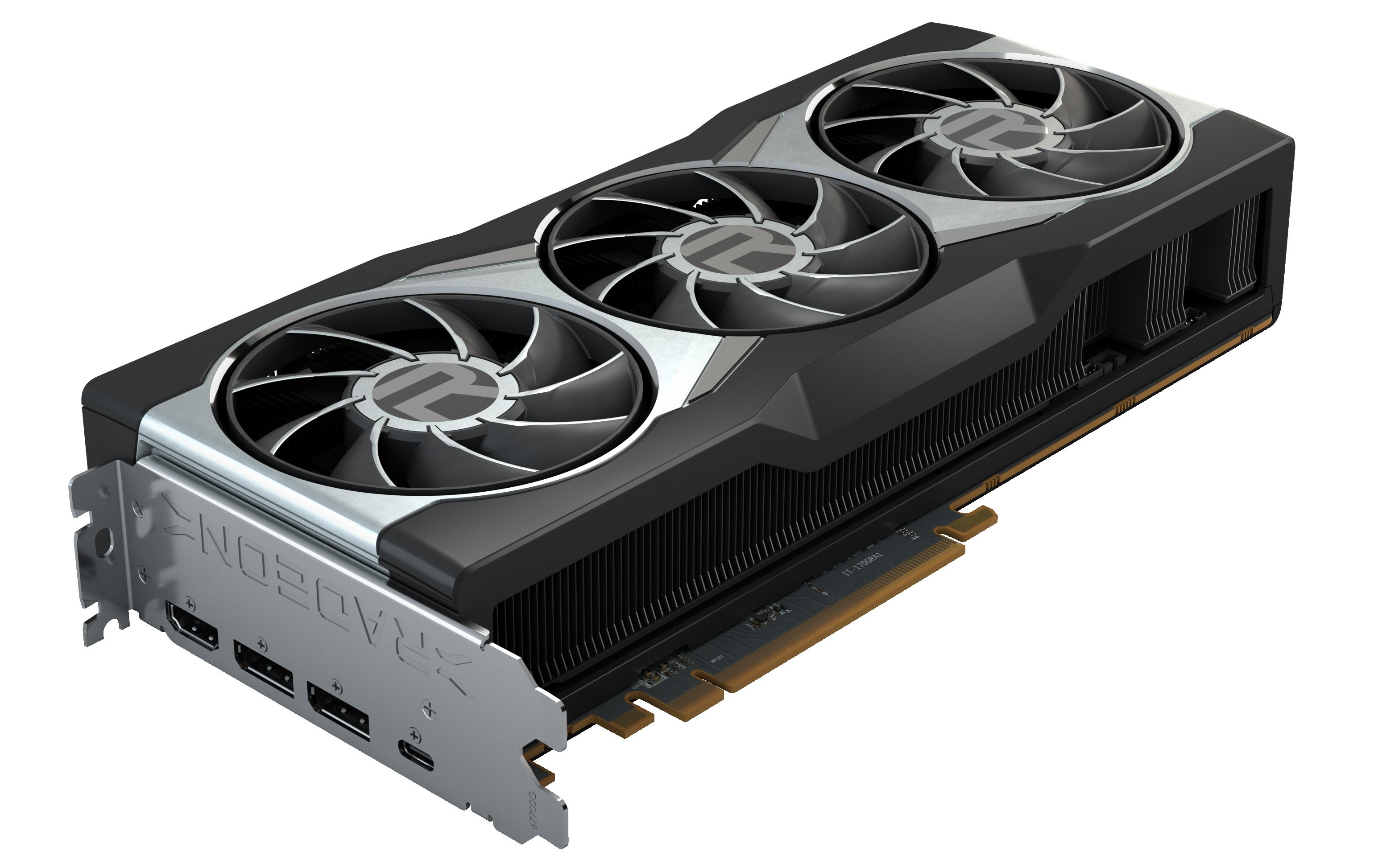
This card will most likely have 24GB of GDDR6 memory (due to the 384-bit bus) and it seems that Angstronomics has already had a chance to see the reference card (or rather, probably 3D renders of it). It’s said to utilise a three-fan cooler similar to the Radeon RX 6900 XT, but a bit taller. It’s said to be accented by three red stripes next to the power connectors.
And heads up: the interesting information is the power supply configuration – it is said to still consist of two eight-pin connectors. This is important. On the one hand, this card won’t need a new power supply or new cabling or adapters (while with high-end GeForce RTX 4090 you can probably expect to need ATX 3.0 / PCIe 5.0 power supplies, or at least “dumb” 12pin adapters).
But besides that, two connectors should mean that the TDP will be “only” 375 W at most. The eight pins give 150 W each, and according to the specifications, 75 W can be drawn from the slot on the board (in reality it’s slightly less, because the graphics draws from the 12V branch, where the limit is somewhat lower, but this seems to be ignored most of the time). However, it’s possible that the GPU will simply draw more than 150 W from the cables, which has sometimes happened before, so the TDP may yet be higher than 375 W. Of course, non-reference cards can have higher TDP and three 8-pin power connectors. A TDP of 375W would probably still be relatively “good” in the end – if you ask it’s still disgustingly more than what we thought was a reasonable limit (250–300 W) just a few years ago, but this would still be better than the 450 W power draw Nvidia is said to be planning for the GeForce RTX 4090, not to mention the rumours of an 800W Titan card.
Cheaper version with 10 752 shaders, 20 GB memory
Angstronomics mentions that the Navi 31 will also be sold in a partially cut-down (deactivated) configuration as usual, harvesting defective or bad-bin chips. This card (Radeon RX 7800 XT? RX 7900?) is supposed to have only 42 WGPs (84 CU) active, which would be 10,752 shaders. There memory subsystem will also be a cut-down, the bus will only be 320-bit, so the card should probably carry 20 GB of GDDR6 memory. With this, the Infinity Cache will also be reduced to 80 MB. In fact, only five MCD chipsets should be active (although the sixth one might still be physically present, we kind of doubt AMD would produce a separate GPU pattern with just five MCDs present).
Navi 32: still chiplets, but no longer 1-hi, mobile high end
So far we have discussed the most powerful Navi 31 variant, but Angstronomics also provides data for cheaper variants. The Navi 32 (“Wheat Nas” or also gfx1101) will still be a chiplet GPU produced in the same manner as the Navi 31. Its 5nm GCD chiplet, however, has only 30 WGP (60 CU) and thus 7680 shaders / FP32 units. It will be divided into 3 shader engines and 6 shader arrays. This GPU has a 256bit bus so it will probably carry 16GB of GDDR6.
It is to consist of one 5nm GCD with an area of only about 200 mm² and four 6nm MCDs, which will be the same as the Navi 31 (37.5 mm²), so there are some cost savings thanks to design reuse. This GPU will only have 64MB of Infinity Cache due to the bus width, again this is less than the 96MB capacity of the Navi 22 chip. Here, AMD is also considering or has considered a 1-Hi variant with twice the capacity, but due to the cost of production it may end up not going into production at all.
This GPU will be the most powerful version of RDNA 3 that will ship in laptops, where it will cover the very high-end segment (Navi 31 is not planned to be used in notebooks). The launch of this chip is not due until 2023 – Radeon RX 7000 laptop graphics based on it will probably be revealed at CES 2023, and the desktop version probably won’t come out before the end of the year either.
Navi 33: cheap 6nm version, targeted at laptops
The third, cheaper variant, the Navi 33, stands out. As we already knew from previous leaks, it is no longer chiplet-based but monolithic, made up of a single 6nm silicon. Its area is reportedly 203 mm², but it still contains 16 WGPs (32 CU) or 4096 shaders. These are in 2 shader engines and 4 shader arrays.
This GPU will be significantly smaller than the 7nm Navi 23 with 2048 shaders (which powers the Radeon RX 6600 XT, RX 6650 XT cards) while simultaneously doubling the unit count to 4096 shaders, which again is pretty noteworthy. However, it still only has a 128-bit bus, meaning it could probably use 8GB of GDDR6 memory in the cards AMD is planning. Its Infinity Cache is only 32 MB, which is pretty low. So there is a lot of question here too as to what kind of performance will AMD be able to achieve. Previously, it was speculated that this GPU could perform up to around Radeon RX 6900 XT (but probably only at 1080p or at best at 2560×1440 pixels). But with this level of cache and memory bandwidth, that seems pretty unlikely.
However, it could be a pretty cheap GPU, given the size on a relatively cheaper 6nm process (cheaper compared to 5nm and 4nm). According to Angstronomics, the performance will be higher than Intel’s fastest Arc generation Alchemist graphics (by which they mean the ACM-G10 GPU, also with 4096 shaders and on a 6nm process), but its manufacturing cost is half that (Intel’s chip is 406mm²) and it will achieve that performance with less power draw.
The Navi 33 design is said to be very much aimed at laptops, which are even supposed to be the primary target. Thus, mobile Radeons with Navi 33 could be relatively widespread, or at least that’s how AMD would like it (we’re afraid that in reality, the gaming notebook segment is almost dominated by Nvidia and Radeons are hard to push to OEMs’ designs). Interestingly, this chip is said to be pin-compatible and can be fitted on laptop boards designed for Navi 23 GPUs – Radeon RX 6600M, 6650M, 6650M XT and maybe even RX 6600S, 6700S and 6800S. This might make it a bit easier to achieve notebook design wins with it.

Desktop versions will of course also exist. However, the focus on laptops could mean that the GPU will only have a PCIe 4.0 ×8 interface (Navi 31 and 32 will hopefully be PCIe 5.0 ×16, but Angstronomics does not provide these details yet), and it is questionable whether there will also be some limitations on the number of video outputs or video encoders, as occurred with the Navi 24 chip in Radeons RX 6500 XT / RX 6400.
Small chips thanks to RDNA 3 architecture streamlining
It has already been mentioned that the 256 RDNA 3 shaders (1 WGP) reportedly require (likely on a 6nm process) a slightly smaller area than the 128 RDNA 2 shaders. AMD is said to have focused mainly on area efficiency and thus cost when designing the RDNA 3 (gfx11) architecture. The pipeline and CU were optimized in this direction, which for example meant removing legacy features (there is speculation about a legacy geometry pipeline being physically removed).
One of these optimizations is to be the “OREO” technology. This acronym has appeared in leaks before thanks to Linux drivers and stands for Opaque Random Export Order. It is a pipeline change compared to RDNA 2, which executed shaders in an Out-of-Order style, but then they had to be put back in the correct order in a special Re-Order Buffer. In the RDNA 3 architecture, the next processing stage (Blend) has the ability to accept the results of shaders out-of-order and then outputs in-order itself, eliminating the need to have that ROB in front of it and saving some unit area.
Another slimming down that is mentioned is the performance reduction in FP64 calculations – instead of 1/16, these operations will now run at only 1/32 ratio.
The slimming down is also perhaps the reason for the reduction of the Infinity Cache compared to the previous generation. By the way, AMD internally refers to it as MALL Cache – Memory Attached Last Level Cache (since it is associated with memory controllers). In the RDNA 3 generation, the company builds this cache from blocks that have half the capacity compared to the previous generation. This is probably to maintain full bandwidth even after the cache has been halved in size. This probably shows that the bandwidth component of Infinity Cache is very valuable for overall GPU performance, while the capacity was negotiable.
AMD has previously reported that the algorithms deciding which data to hold in Infinity/MALL Cache have been changed for RDNA 3 chips. This is perhaps an effort to get the most performance out of the smaller capacities. Hopefully, it will turn out that the larger capacities of RDNA 2 GPUs were not so necessary after all and AMD did not incur a grave disadvantage on the new generation RDNA 3 with this capacity reduction.
Source: Angstronomics
English translation and edit by Jozef Dudáš
⠀

