Intel’s Alder Lake CPUs are poised to be the biggest hardware event this year. Intel has unveiled the core architecture of these CPUs and we have analysed the details and new improvements inside. There’s promise of huge performance and one of the biggest architectural leaps in x86 processors, for the first time with six parallel decoders and further IPC increases, showing Intel taking the same path as Apple’s highly effective cores.
As we’ve highlighted the advancement of decoders which symbolises how the Golden Cove architecture is going in the direction of widening the core, we can do similarly with backend execution units, although in their case the direction may not be as noticeable. However, the IPC-increasing policy is very noticeable in the size of out-of-order buffers and queues. The processor can hold much more operations in these structures thanks to their enlarging, so it will not stall during various delays (for example, when data is missing and needs to be loaded from RAM, or in cases of branch mispredicts) as much. These buffers also serve for optimizing performance by allowing CPU to perform operations in an order different from the program code order.
The latter is the very nature of what is called “out-of-order Execution” architecture: the core reorders the instructions it is processing in order to fit as much work as possible into a single cycle, trying to utilize as much of its execution units at once as possible. This reordering allows to exploit instruction-level parallelism in code even when data dependency between instructions would block a simpler “in-order” core from doing so because the following instruction has to wait for the output of the preceding one or because it has to wait for data being fetched from memory. out-of-order core looks ahead into the instruction stream for independent instructions that already have their inputs ready and executes those in advance. This greatly improves the ability to utilize four or six operations per cycle in these wide microarchitectures and is the main source of IPC increases in modern processor cores. In order to achieve higher and higher IPC through out-of-order execution, the CPU core has to be provided visibility into a larger and larger “window“ of code that it can look for independent operations and perform the reordering over. The size of this “window” is determined by the length of the so-called Re-Order Buffer (ROB) queue, in which the reordering is taking place.
It’s exactly the Re-Order Buffer that sees perhaps the second most significant increase in resources in the Golden Cove core, after the Fetch & Decode Stage power-up. And it is likely no coincidence that Re-Order Buffer depth is another thing that is exceptional in Apple’s ultra high-IPC cores. Intel is again going down the same path. While in Skylake the ROB was 224-entries (μOPs) deep and Ice/Tiger/Rocket Lake (the Sunny/Willow/Cypress Cove architectures) have increased it significantly to 352 μOPs, the new Golden Cove core comes with another large bump: it’s ROB now has 512 entries.
It has to be said that Apple’s microarchitecture is still quite ahead, it is believed to have up to 630-deep ROB (roughly). The relative jump in depth in Golden Cove is regardless very large and most spectators likely didn’t expect this much. Moreover, we can expect further deepening in the following updated microarchitectures in the future. This increased ROB depth can’t be had for free, it comes at the cost of more transistors and also more power usage. And due to that it is likely quite difficult to implement it in an energy-efficient way. Interestingly, AMD’s Zen 3 microarchitecture still relies on ROB that is merely 256-entry deep (while still achieving IPC on par or better than Intel’s Tiger Lake with 352-deep ROB—this shows you how CPU core performance is never determined by one isolated parameter only). But it is likely that AMD is going to increase the ROB “window” too, in their future microarchitectures.
Increased performance potential in the backend
As with the case of Fetch and Decode, the increase in ROB depth goes hand in hand with other increases, namely in the counts of execution units in the backend of the core. It makes sense to increase these resources together in balance, as the larger window is what allows the core to actually utilise more parallel execution units.
Intel keeps using their traditional scheme (that goes all the way back to their first out-of-order core, P6 a.k.a. Pentium Pro) where execution units are grouped behind a set of execution ports and the CPU scheduler in the core dispatches μOP to these ports. While execution units behind different ports can be used simultaneously, units behind a single port can not. The scheduler itself is a single unified one simultaneously serving ALU ports, Load-Store (AGU) unit ports and also SIMD/FPU instructions (whose units are located on the same ports used by scalar ALU units). Competing cores from ARM but also AMD have the core split into separate parts for scalar ALU instructions and for AGU units and a separate pipeline for FPU and SIMD operations that can have its own scheduler. Interestingly, this is what Intel actually uses in their “little core” microarchitecture used in Alder Lake (Gracemont), it also uses the split core design, while Golden Cove does not.
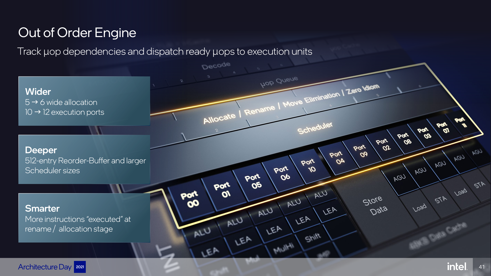
Golden Cove has increased the number of parallel ports to 12 from 10 used by the previous architecture (in Ice/Tiger/Rocket Lake; the Skylake core was using 8). This increases the number of operations that the CPU can simultaneously issue in a burst from its scheduler (but as we have seen, the previous pipeline stages are limited to 6 μOPs per cycle so it is not possible to sustain the 12 μOPs throughput in backend outside of bursts)
Five ALUs for the first time
The ALUs or (integer) arithmetic logic units are located behind ports 0, 1, 5, 6 and behind the newly-added port 10, which adds a fifth ALU to the four that have been present in past cores. This also makes Golden Cove the widest-yet processor core in the realm of x86 architectures. For comparison, AMD’s Zen to Zen 3 cores have only four ALUs, but Apple has famously used six ALUs for some time now.
All five ALU ports also support the LEA (Load Effective Address) instruction, which is very common in x86(x86-64 code. Its original purpose is memory use, but it can be exploited for doing arithmetics and compilers routinely emit it for this purpose. Golden Cove can do LEA on all five ports with 1-cycle latency, which means it is done by the next cycle.
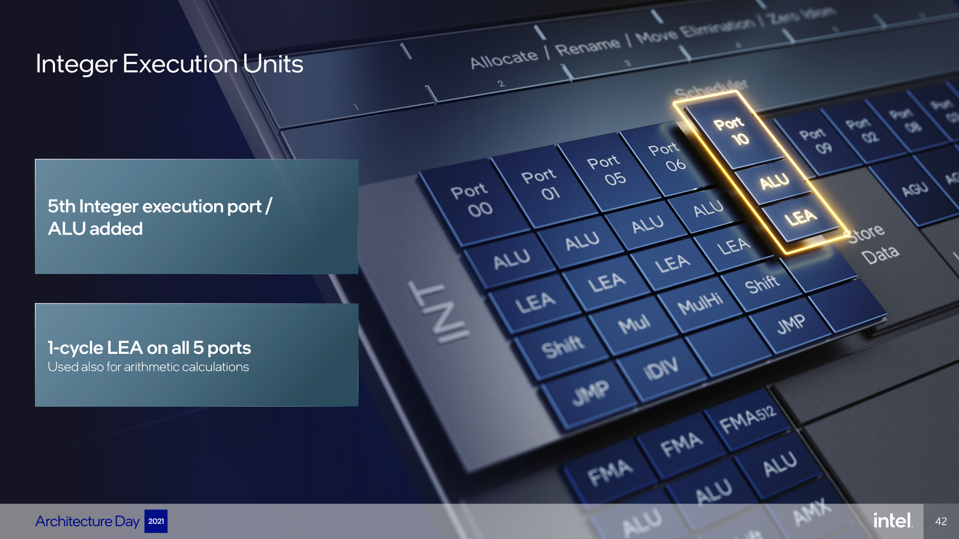
While all five ALUs can do simple operations, more complex instructions have more limited throughput. Integer multiply is handled by only two ports, as are bit shifts and branching (JMP) is also handled by only two ports, which means Golden Cove can process two branches per cycle (same as Zen 3). Integer division is only provided by a single port/unit.
Stronger AGU subsystem for better memory performance
Load-store units or AGU (address generation units) perform reads and writes to the RAM, or more precisely to L1 data cache and they have also been strengthened in Golden Cove. Instead of four AGUs, there are now five (ports 2, 3, 7, 8 and the fifth has been added on the second newly introduced port 11). Three units perform Load operations and two are for Store operations, which means that Golden Lake supports three reads and simultaneously two writes to L1 cache. The maximum read and maximum write ops per cycle are the same as for AMD Zen 3, but there is a crucial difference: Zen 3 only has three AGUs and can only do three memory operations in total—three reads, or two reads and one write or one read and two writes. Besides AGUs themselves, the Golden Cove core has two separate ports for Store Data operations (ports 4 & 9), which is something carried over from previous cores.
It is however not just the number of read/write operations possible per cycle that we should look at, what is also important is the bandwidth. And Golden Cove provides up to double the bandwidth achieved by Zen 3. The regular client version of Golden Cove core that will be used in Alder Lake should be able to perform three 256-bit loads (256 bits corresponds to the width of an AVX/AVX2 register) from L1 cache per cycle, which gives the bandwidth of 768 bits/cycle, a 50% improvement over previous core. Server variant of Golden Cove with AVX-512 support will alternatively be able to perform two 512-bit reads (512 bits matching the width of an AVX-512 register) per cycle, allowing the core to feed its execution units with up to 1 Kb of data per cycle.
L1 cache itself was not changed in the manner of associativity or capacity, which is still 12-way 48KB as introduced in previous Ice Lake/Sunny Cove architecture. The memory subsystem performance was however boosted by other means. L1 cache fill buffers were increased from 12 to 16, L1 cache prefetching was increased and L1 data cache TLB was increased from 64 to 96 entries. All these tweaks should improve memory performance. The processor should also see better performance when it needs to fetch data from further levels of memory subsystem in the case of TLB miss, thanks to the change of the number of page walkers to four from previous two (Intel however is somewhat less aggressive than their competitor here, because AMD moved from two to six page walkers in Zen 3).
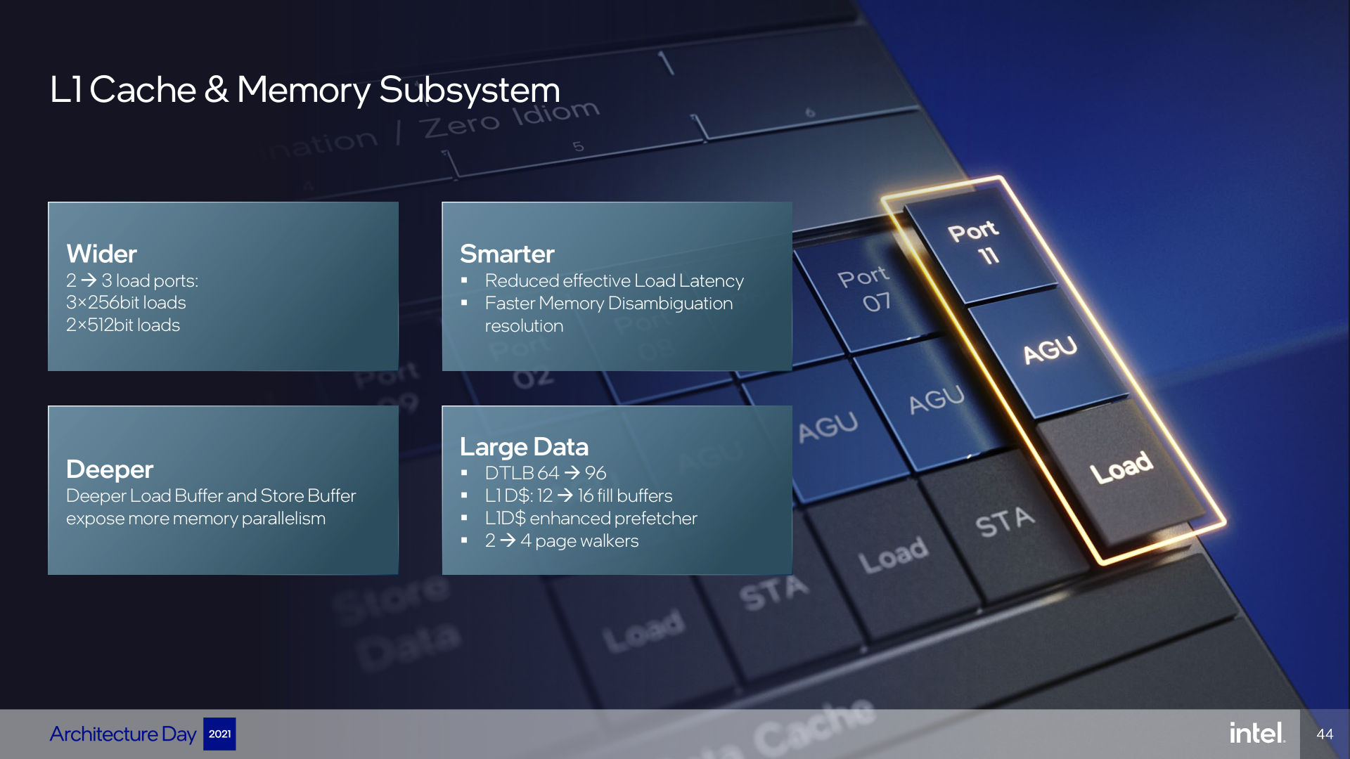
Further, Store and Load Buffer queues for the reads and writes to RAM (through L1 cache) have been deepened, but Intel is not disclosing the exact values. Another improvement is in the performance with which the core handles memory disambiguation (determining the dependencies between memory operations, which allows their faster execution out-of-order). The net result of these optimizations is lower effective L1 load latency, according to Intel.
The L2 cache has been improved too. Particularly it can now handle more outstanding cache misses (requests of data from further levels of memory hierarchy when they are not found in L2). While older cores could have up to 32 outstanding misses in flight, Golden Cove increases the limit to 48. This should allow one core to sustain utilization of higher absolute memory bandwidth from RAM, which is by the way another parameter, in which Apple cores are considered superior to AMD or Intel, possibly helping to their high effectiveness (IPC). Maybe Golden Cove will get closer, thanks to this. L2 cache should also have more effective prefetching, which also supports throttling based on feedback, so that it limits its bandwidth usage in cases where it is needed for other operations. There should be other improvements too, for example Intel mentions new Full-line-write predictive bandwidth optimisation.
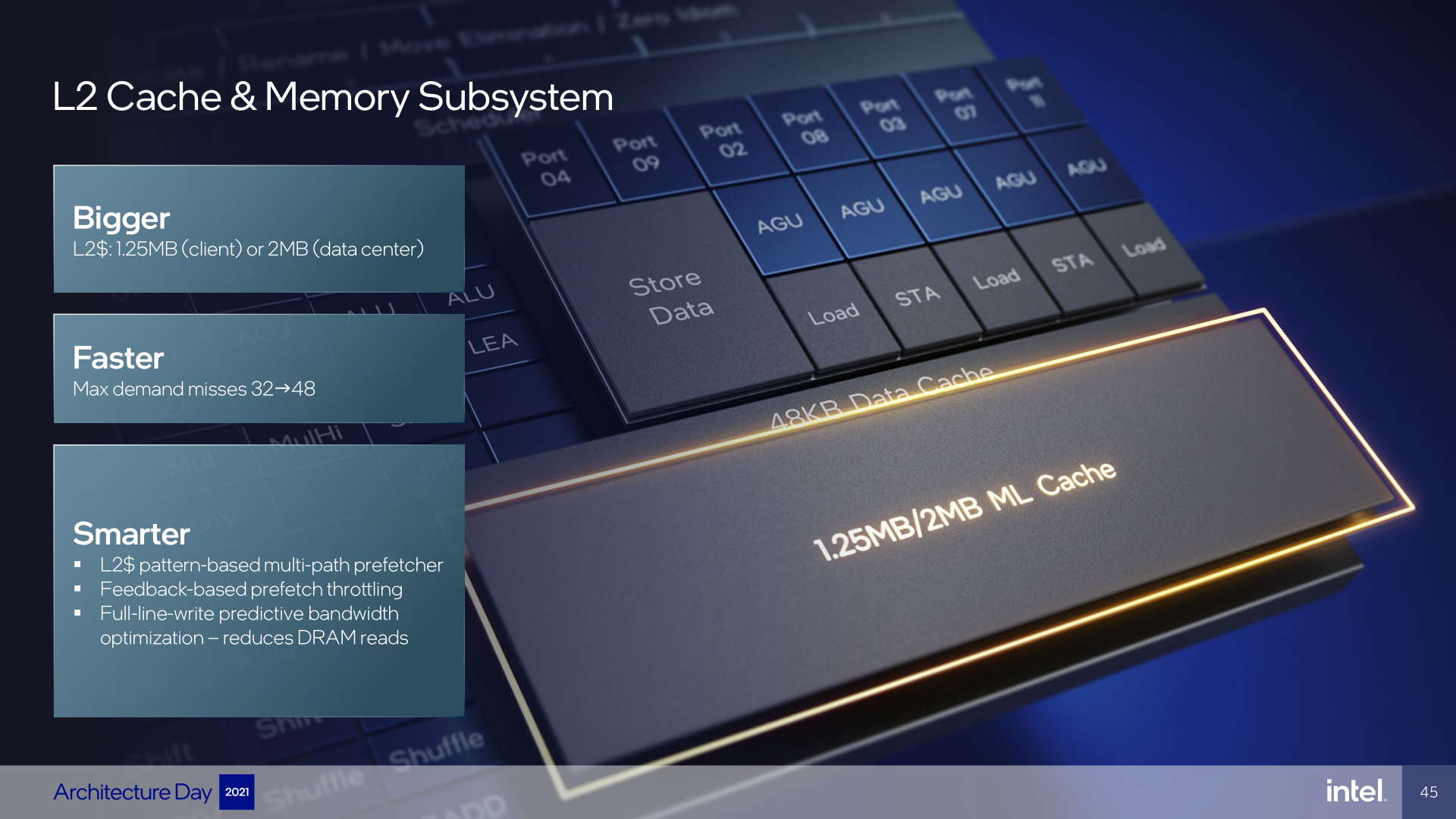
L2 cache capacity is unchanged from Tiger Lake/Willow Cove at 1.25 MB per each individual core (which will however be a large increase compared to the desktop Rocket Lake processors that use smaller 512KB L2 cache—though it seems there has not been a large observed impact from this in Tiger Lake). The server version in Xeon “Sapphire Rapids” processors will add further 768 KB, ending up with 2 MB total in each core.
The article continues in the next chapter.