


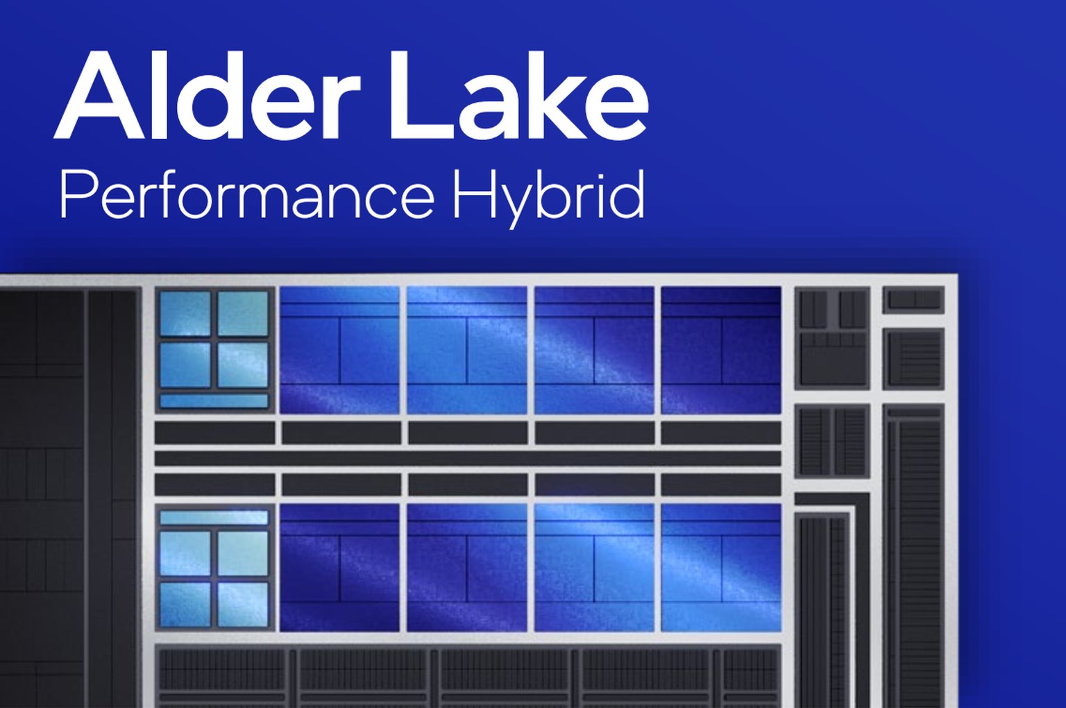
Intel’s Alder Lake CPUs are poised to be the biggest hardware event this year. Intel has unveiled the core architecture of these CPUs and we have analysed the details and new improvements inside. There’s promise of huge performance and one of the biggest architectural leaps in x86 processors, for the first time with six parallel decoders and further IPC increases, showing Intel taking the same path as Apple’s highly effective cores.
As already mentioned, due to not using split FPU design, the FPU and SIMD units (that handle not just floating-point but also integer instructions, despite traditionally being put into the same bag with x86/FPU ops) are fed from the same scheduler as integer part of the core, but furthermore, the FPU/SIMD units share the same ports with integer ALU units. The parallelism of FPU/SIMD units is weaker though, all the operations are only handled by three ports in total—ports 0, 1 and 5, same as in previous coes.
This use of just three ports might sadly somewhat limit the ability to improve the IPC in programs by interleaving SIMD and scalar integer instructions (a strategy that might be successful in ARM or AMD Zen processors). Less ports used to expose the underlying units also leads to more potential scheduling conflicts. For example: while it can be very useful that the Intel cores have the ability to perform two shuffles per cycle, this leaves just one more available port that could perform an additional operation in the same cycle. So while the Golden Cove is in theory a wider core, it is possible that Zen 2 or Zen 3 could achieve higher IPC (instructions per cycle throughput) for certain instruction mixes.
All the three ports contain vector ALUs for integer SIMD operations, while permutations (shuffles) are available on two ports (1, 5), shifts as well (0, 1) and there is just one floating-point divider. The core should be able to perform two or three 512-bit AVX-512 operations per cycle, depending on their type, if working with integer data types. When doing floating-point math, the maximum is two 512-bit FMAs or up to three 256-bit FMAs.
The FMA unit is on all three ports, but as in the previous cores (or at least the server variants thereof), the inner working is such that the the first two ports only have a 256bit FMA units that can do either an 256-bit AVX/AVX2 op per cycle individually, or they can couple to perform a single 512-bit AVX-512 instruction per cycle together. The third FMA unit on port 5 is natively 512-bit wide allowing it to perform one (second for the whole core) AVX-512 instruction per cycle. We do not yet know if this unit will be exclusive to the server variant of the core (Sapphire Rapids) or the HEDT derivatives, but it is a likely possibility. If so, the client core will not be capable of three 256bit FMAs per cycle but instead only two.
What is new in Golden Cove is that Intel has added an alternative FADD unit to ports 1 and 5, which does floating-point SIMD adds with a lower latency and particularly with lower energy consumption compared to the use of the heavyweight FMA units for this task. The processor should prefer these units when possible.
FP16 calculation support
AVX-512 instructions have gained a new ability in the Golden Cove core: to perform operations with 16-bit FP16 data type (where the total computation throughput should be double compared to using FP32). This on one hand further fragments the ecosystem of AVX-512 instructions user base with a new extension, but the FP16 ops should be highly useful for tasks like AI processing and perhaps even for multimedia processing.
This seems to be the biggest enhancement in the SIMD capability together with adding the FADD pipelines. Otherwise the theoretical computation capacity has seemingly not been expanded (unless Intel failed to disclose some additional secret changes), but the IPC of programs using them should still go up thanks to the improvements in the other parts of the core.

AVX-512 hard disabled in all Alder Lake chips?
The advancements in AVX-512 are in a way moot though. Why? As Alder Lake has embraced the big.LITTLE concept, AVX-512 support has to be disabled, as it is in conflict with the “little” Gracemont cores, which do not support these instructions. Without some special trapping/exception handling, any program attempting to use an AVX-512 instruction would instantly crash if it happened to be running on the Gracemont core. Even if that was solved, AVX-512 code would be useless in multi-thread applications, because they would be limited to run on just the big cores and it looks like in multi-threading, the little cores actually represent a very significant part of the overall throughput performance of Alder Lake. This means that a program would in most cases lose more performance by not being able to utilise the little cores than it would be able to gain from utilising AVX-512 on the remaining big cores.
For these reasons, Intel has decided to completely disable AVX-512 on the consumer version of Golden Cove core used in Alder Lake processors, despite this support being present in the silicon. The cores will only support AVX and AVX2. Furthermore, even if you disable all the little cores, this won’t allow you to turn AVX-512 back on, the support is said to actually be fused off. This is unfortunate for software developers, as previously there have been hints that for such uses, AVX-512 could be reenabled by switching little cores off. Intel seems to have decided to not allow this in the end, possibly to avoid confusion and extra complexity.
You will only be able to use AVX-512 in the server variants of Golden Cove employed in Sapphire Rapids and derived HEDT processors. Intel might in theory make special Alder Lake SKUs for the mainstream LGA 1700 socket that would not have any little cores enabled and thus could support AVX-512. But we think this is unlikely as this would look a bit awkward in Intel’s product segmentation scheme which the company likely wants to avoid.

Many times before there have been complaints that it is Intel’s own politics that is the biggest hurdle in AVX-512 adoption. This latest step is the biggest self-sabotaging of this technology yet. Ironically, Intel is torpedoing the feature that it has presented as its competitive advantage before just two years after AVX-512 finally made its way into mainstream client CPUs with Ice/Tiger/Rocket Lake processors, now taking it away again. This will make it hard for software developers to employ these instructions as the installed base of capable computers remains small. Big.LITTLE turns out to be bad news in this regard. In yet another strange development, there are now some (so far unofficial) reports that AMD’s Zen 4 architecture might actually start to support AVX-512, just as Intel is stepping away from it. Competing AMD processors might actually become the go to product if you require the support of AVX-512, once Intel’s exclusive sales point.
Some further instructions set extensions that prior big cores used to support might have also been disabled in Alder Lake’s Golden Cove cores to make them instruction-set compatible with the little Gracemont cores. These additional sacrifices hopefully won’t be as problematic (though if you specifically used them for some optimization in your code, you no doubt won’t be amused).
Which however has been retained from AVX-512 even in the consumer client version of Alder Lake is the VNNI instructions. These have been reduced into a possibly somewhat less performant version employing just the 256bit YMM registers for AVX/AVX2 instructions instead of using the 512-bit ZMM registers. This allowed them to be implemented in the little core as well and thus this VNNI256 variant will be available on Alder Lake.
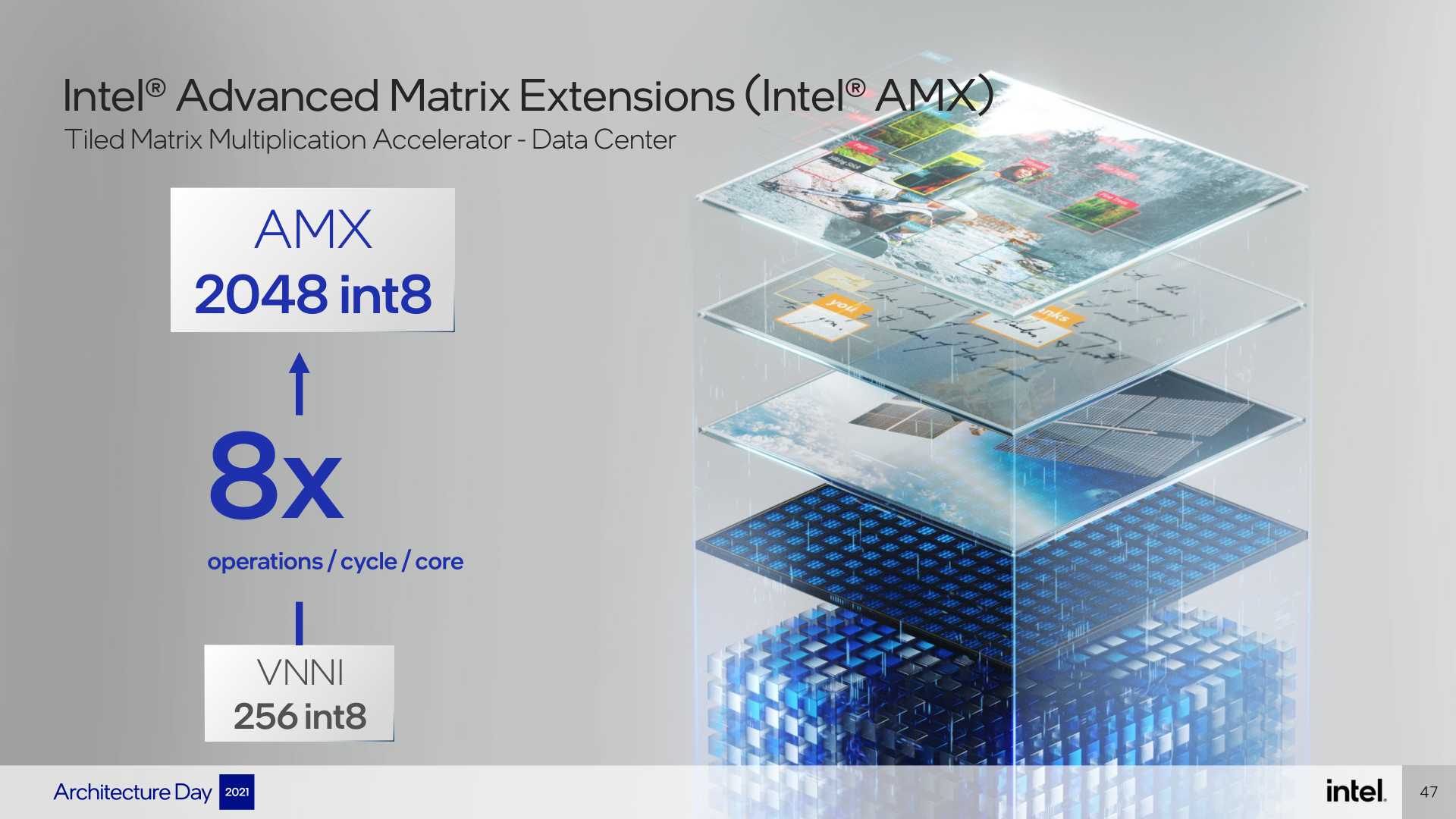
Advanced Matrix Extensions (AMX)
The server variant of Golden Cove in Sapphire Rapids Xeons will offer one extra feature, besides its AVX-512 support. And that is the AMX instruction set extension, which will not be physically present in the client variant of the core (Alder Lake).
AMX is a set that performs 2D matrix multiply operations with a very high level of parallelism, thus achieving very high raw performance. However as it happens, this performance will be applicable to a limited amount of uses, basically these operations are useful for AI acceleration. You might think of these AMX units as a similar accelerator as tensor cores in Nvidia GPUs. Golden Cove has one AMX unit present in it, which is exposed on port 5.

The AMX instructions perform the matrix multiply using INT8 data type. The calculations are performed with 1024-bit registers which are new in this microarchitecture and the core contains eight of them (T0 to T7). One register should contain 128 of INT8 values and the unit will achieve up to 2048 calculations per cycle on one core with them. If we made a mistake somewhere or misread Intel, this means 2 TOPS of AI performance on one core at 1GHz clock speed or 8 TOPS at 4 GHz etc.
The article continues in the next chapter.


