

This year, Intel is expected to complete its 2nm and 1.8nm production nodes (designated Intel 20A and Intel 18A) in culmination of their plan to develop five nodes (Intel 7, 4, 3, 20A and 18A) in four years and catch up with the technological lead of TSMC. Now, the company has revealed the next step that will come after this cycle, and a roadmap for enhanced nodes, reminiscent of the plus sign suffixes familiar from 14nm node era.
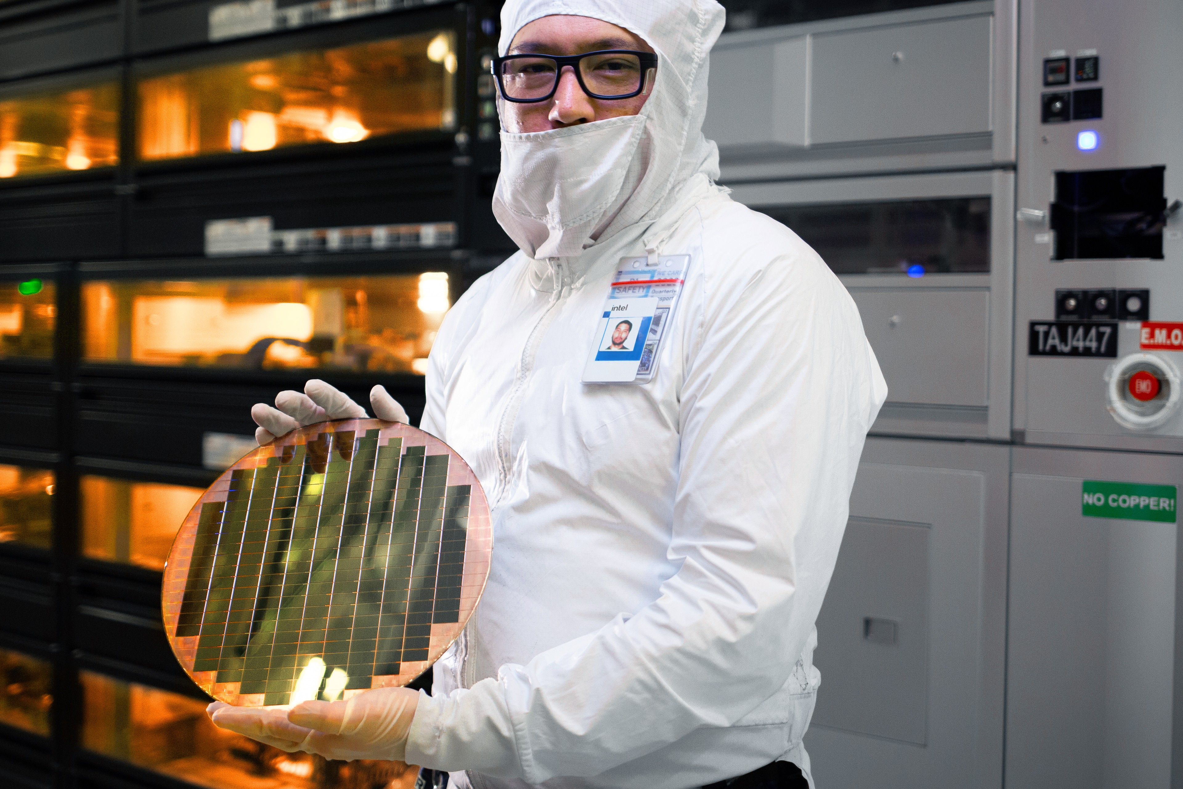
Following the release of the Meteor Lake processors, Intel can now report that it has chips made with its first EUV process (Intel 4) in market. Its successor, Intel 3, is ready for production now, according to the company, but its own 3nm product (Granite Rapids and Sierra Forest server processors) has not yet been released. Intel’s 20A and 18A nodes that introduce GAAFET transistors (Intel calls them RibbonFETs) and PowerVIA technology will follow this year.
These technologies could be groundbreaking, comparable to the advent of FinFET transistors. Intel 20A should be ready in the first, Intel 18A in the second half of this year – but it is possible that it will not be used in products until next year.
Intel 14A with High-NA
Last week at the Direct Connect conference, which was dedicated to Intel’s foundry business, the company has announced the next step following the 2nm and 1.8nm nodes. This will be the node designated Intel 14A. The name should mean 14 Angstroms, so it can arguably be called a 1.4nm process.
What are Angstroms / what does Intel 18A mean?
Angstrom with the A symbol is a less commonly used unit corresponding to exactly one tenth of a nanometer. 20 A therefore means 2 nm. The so-called Angstrom era nodes, as Intel calls them, are labeled, for example, Intel 20A or 18A, implying that they are a 20A = 2nm and 18A = 1.8nm node respectively.
Keep in mind, however, that these nanometer numbers are essentially arbitrary for all companies, disconnected from any physical reality (note that we do not mean that pejoratively here). The structures in a chip are always larger, and the series of these numbers denoting process nodes are meant to reflect relative progress against previous technology, not absolute dimensional parameters.
At the same time though, these numbers can also be bent and inflated by marketing, of course.

There is no data on how much better this process should be compared to Intel’s 18A technology, nor has Intel published transistor density projections or structure dimensions data. However, it has been reported that the 1.4nm node will be the first to apply High Numerical Aperture (High-NA) technology.
What is High-NA technology?
High-NA is an extension of current EUV lithography to further improve the ability of extreme ultraviolet light to form extremely small structures on a chip.
It does this by using anamorphic optics with larger mirrors to increase the numerical aperture from 0.33 to 0.55, which should enable the creation of 1.7 times smaller (41% smaller) transistors. Of course, this is very difficult to implement and there are also disadvantages, as this reduction also halves the area that the High-NA EUV machine patterns on the wafer. So to fill the whole wafer requires twice as many patterning steps. It also seems to reduce the maximum chip size, so for instance large high-end GPUs will inevitably have to use interconnected chiplets (tiles) from now on.
It’s interesting that the advent of EUV (as late as on 4nm chips/Intel 4 node) was much delayed in Intel’s fabs, but according to this, teh company will actually deploy ASML’s Twinscan EXE high-NA systems as the first player in the industry. This will likely increase manufacturing costs but should improve process node parameters. An alternative to High-NA is to use double patterning with current EUV technology, which is also technically feasible. Intel states that this is a fallback option and the company is prepared to switch to it if an aggressive High-NA deployment turns out to be too risky, accompanied by problems that would block timely rollout of 1.4nm technology.
Realistic arrival in 2027
This technology will not be in production for a considerable amount of time. The so-called risk production, which is a test production at the stage when the technology is not yet fully tuned and the yield is low, is to occur at the end of 2026. Commercial deployment will therefore be in 2027, it is also possible that real 1.4nm processors will be sold at the end of, or at best in the second half of 2027.
There is, of course, the possibility that problems will occur and deployment will be delayed. So in practice, Intel’s 14A node should probably compete in the market with TSMC’s 2nm process. And it’s possible that it will roughly match it’s parameters as well (as opposed to parameters of eventual TSMC 1.4nm node). It is not completely ungrounded to suspect that the numbering of Intel’s 3, 20A and 18A nodes may be a bit ahead of reality compared to the nanometer numbers of TSMC’s processes.
Samsung also has a 1.4nm process planned for roughly 2027, but in this case it’s also possible that the technology will realistically compete with TSMC’s 2nm node.

Improved nodes with pluses
Intel also announced the return of incremental node improvements that were historically marked by a plus, such as 14nm+. This seems to have in fact been happening with the Intel 7 node (the variant used for Raptor Lake is said to have an unofficial designation Intel 7 Ultra), but Intel has ceased to explicitly label these incremental technology tweaks, probably because the extreme amount of “pluses” that got tacked on the 14nm process in the ended up giving this practice a bad name. Instead of denoting the advancements in the technology, it ended up being seen as a symbol of Intel’s stagnating.
The 14A node has an improved version 14A-E already announced. The “E” will denote some sort of additional capability of the nodes, which for Intel 14A-E is supposed to be the ability to operate at higher voltages and temperatures (and thus achieve potentially higher clock speeds – it could be something similar to TSMC’s HPC processes marked with an “X”).
This node is supposed to have some improvement in performance or power efficiency even in general, without using the higher voltage capabilities. However, the improvements for the E variants are only supposed to be in low single digit percentages. In addition to Intel’s 14A-E, such an improved variant is also expected to be available on top of the base 16nm node (16-E) and based on the 3nm node (3-E).
In addition, there will also be enhanced nodes marked with “P“. This simply means Performance, these processes will deliver higher improvements in power efficiency and performance compared to their basic technology, typically there’s going to be some 5–10% improvement. Basically it will probably be in the ballpark of what Intel once designated with those extra plus signs. Improvements won’t go over 10%. Intel stated that such an improvement would be designated as an entirely new node (probably with a smaller nanometer/angstrom number.
These improved P versions are now planned for the 3nm node (it will follow Intel’s earlier 3-E node). Not all of these different technologies will be directly used by Intel processors, they are mainly intended to be available to external foudry customers, providing them with more options.

TSV processes
In addition, a “T” variant will also be developed from some nodes. Currently it was announced for the 3nm node (Intel 3-T and 3-PT, as the suffix enhancements can be combined). The “T” indicates that Through-Silicon Vias technology can be used in the chips, which means channels are excavated through the silicon to create a channel (copper wire) that connects the top side of the silicon to the metal wire layers on the bottom side, so that another one die then be mounted on the chip, in the so-called 3D stacking. This is exactly the technology that AMD (via TSMC’s fabs) is using for 3D V-Cache processors.
Interestingly, Intel’s concept is a little different. While AMD (TSMC) is using TSV combined with bleeding-edge process nodes, Intel wants TSV only for slightly mature nodes, which will eventually be the 3nm node by the time high-end chips or chiplets will be produced on 1.8nm or 1.4nm nodes. Intel’s concept is to place TSVs in a less critical piece of silicon, such as the IO die or SoC tile, which is manufactured by an older process node and lies at the base of the packaged processor, while the performance-critical compute chiplet is manufactured by the latest advanced process and is plaves on top. Therefore, it doesn’t have to have TSVs, those will only be formed in that bottom silicon produced by the older process. If, for example, the Ryzen 7000X3Ds were manufactured in this style, they would have a cache chiplet underneath the CPU chiplet and the TSVs would pass through the cache. This would certainly be better for cooling, but then you would not be able to use the CPU chiplet on its own without additional cache (which is part of AMD’s strategy).

Addition of 12nm process developed with UMC, 65nm Tower Semi technology
But in addition to these Intel-developed advanced nodes, Intel has other technologies in the pipeline that use older and cheaper technology for products that don’t require the best (and most expensive). This will be the recently announced Intel 12 node that Intel will offer in its factories, but it will be developed in collaboration with UMC. And similarly, Intel’s services are to include a 65nm node, which in turn will be from Tower Semiconductor, a company that Intel recently tried to buy but failed to get the deal through market regulators.
These nodes will probably be focused purely on foundry services for external clients. They probably won’t be used in Intel CPUs or GPUs, although they might eventually appear in Intel’s Wi-Fi, Ethernet, chipsets and similar adjacent chip products.
Sources: Intel, AnandTech
English translation and edit by Jozef Dudáš
⠀
⠀