


We are currently waiting for Intel’s new desktop processors (Rocket Lake, later Alder Lake), but it looks like the company is planning much bigger changes for servers. A sample of a Sapphire Rapids server processor and possibly high-end desktop surfaced on the web and it looks very interesting: it is composed of chiplets, some versions should have HBM2 memory inside and a small FPGA has even been found under the IHS.
Sapphire Rapids processors will be primarily intended for servers, and are expected to be released in early 2022 as a successor to the “Ice Lake-SP” Xeons, which should actually be released any time now. Sapphire Rapids are supposed to have 48 or more cores derived from the Willow Cove/Tiger Lake architecture, but with extensions such as higher AVX-512 performance, AMX for AI operations. The processors will move to eight-channel DDR5 memory controller (possibly with official DDR5-4800 support) as well as PCI Express 5.0 support that will include the cache-coherent CXL protocol. And they will be produced in the improved 10nm SuperFin process that proved itself in Tiger Lake, which has reached clock speed of up to 5 GHz thanks to it. We also already know that Sapphire Rapids will use the new LGA 4677 socket.
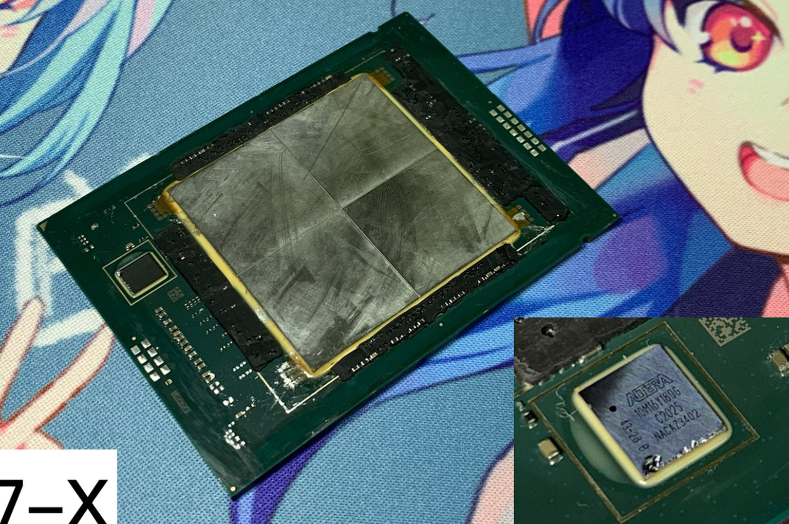
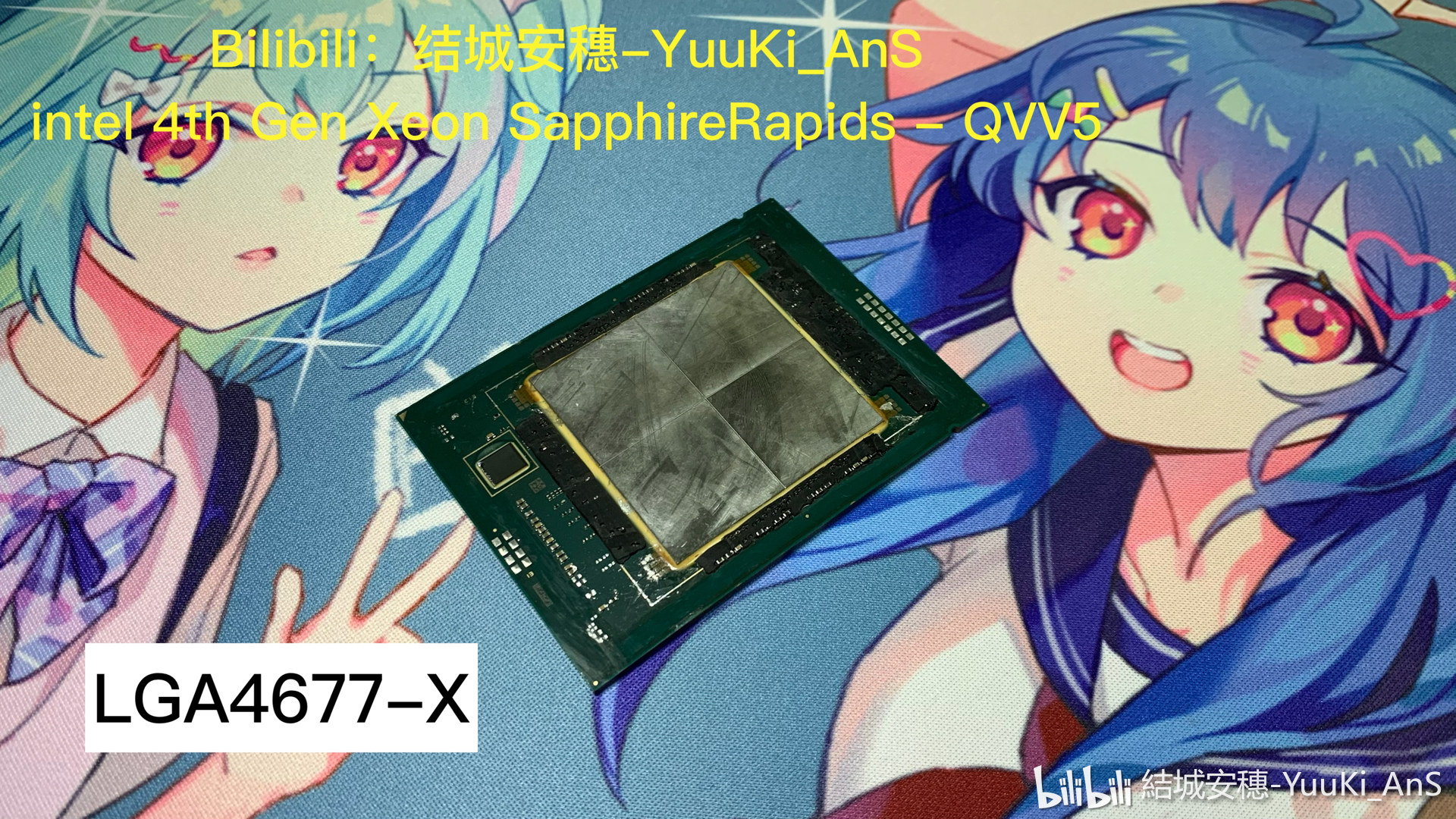
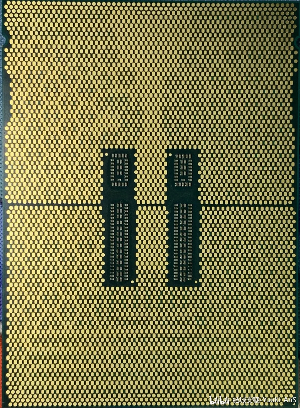
This week, a user YuuKi_AnS on a Chinese web Bilibili showed a photo of the processor that is designed exactly for this LGA 4677 socket. The number indicates the number of contacts on the bottom, so this CPU has even more of them than Epyc and Threadripper processors (it’s really big). According to the leaker, the photo shows Sapphire Rapids, more precisely 1st or even 0th generation ES sample. Although the launch date is still a long way off, Intel has already announced that it has begun distributing samples of Sapphire Rapids to selected partners, which is probably how this photo ended up being taken and leaked.
At first, only photos of the CPU were published, with the leaker likely not knowing its exact specs – the core count could be as high as 56 in the silicon itself, and since some Sapphire Rapids processors are said to contain HBM2 memory, it was possible that those were hiding in this sample, too. The only thing that is clear is the base clock speed, which is printed on the heat spreader even for ES processors. We can read that the CPU runs at 1.30 GHz. Whether a turbo boost is active on top of that and what clock it should reach, is something that is not said on the tin. Tom’s Hardware states that it learned from its own resources that the Sapphire Rapids sample labelled like this (QVV5) should only have active 28 cores – so a large part of the physical cores is likely inactive.

The low clock speed is not surprising or something to be worried (or gleeful) about. ES samples tend to not have specs corresponding to the final processors and they often have poor clocks like this, especially in the early phase. This is especially true for server CPUs with many cores.
There are really chiplets inside
Later though, the same source added another photo where the heat spreader is removed and this is where the fun really begins. We can confirm the rumours that Sapphire Rapids is no longer a monolithic processor. Intel, like AMD, has joined the game of chiplet processors combining multiple silicon dies. But the technology used by Intel might be more advanced. The photo shows four roughly square chiplets, which are fitted side by side with only a slight gap between them, which is unusual.
One can guess that this could be a sign of advanced packaging beinf used. These pieces of silicon could likely be interconnected through EMIB silicon bridges. These are functionally similar to the interposers used with HBM2 memory, but hopefully EMIB could be cheaper technology. Using silicon interposer or EMIB could probably significantly reduce the energy efficiency overhead and latency degradation caused by communication between chiplets on AMD processors that do not use such advanced packaging and simply rely on ordinary organic substrate. It is also possible that Intel has used their Foveros technology, which could mean a separate “IO chiplet” (similar to the one used by Epyc 7002) being hidden under the CPU chiplets that are visible in the photo.
The delid did not show HBM2 memory on the other hand, which means this sample does not employ that technology. It looks like integrated HBM2 memory will probably be a specialized solution and not a part of all Sapphire Rapids processors. If it’s even confirmed that Intel plans to use it in any SKUs.
FPGA: just for the prototype, or permanently?
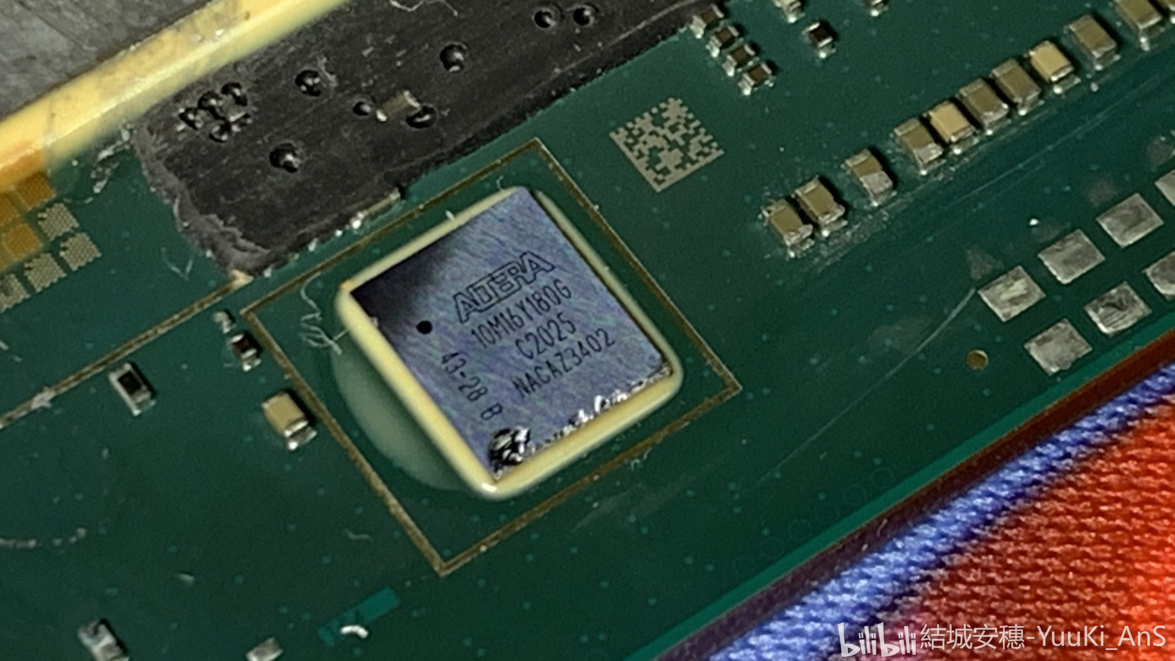
Next to the four CPU chiplets, however, there is one special smaller chip on the substrate on the left (it has a lighter frame drawn around it). This is not a standalone memory chip. Closer-up photo reveals that this silicon is labelled Altera and is therefore an FPGA. We do not know what role it plays. Its isolated location on the side of the processor gives the impression that it likely doesn’t serve as a performance-enhancing accelerator – a larger FPGA would probably be used for that, or there could be a larger number of them.
The FPGA may be used to add some IO technology that the processor lacks by itself – or that is malfunctioning/broken in this silicon revision. In fact, the FPGA could be present purely because this early silicon does not work completely flawlessly and needs some assistance to even start up, which can be realized by this programmable circuit. Although who knows, maybe we’re wrong and in the end this chip will also be in the mass production version. Where it could offer interesting new possibilities.
The silicon area is very large
Even without this, these processors are going to be very remarkable with their chiplet form. This could allow a very high performance to be achieved, because it allows the processor to be given much larger total area than what a monolithic one would allow. And larger area means more space for cores, and therefore more performance potential. Because documentation for the LGA 4677 socket diagrams has been leaked, we know more or less how big the substrate (board) of the processor is. A Twitter leaker/blogger _rogame tried to estimate the size of the chip according to the dimensions of the substrate and found that one die has area of 419 mm², which is actually a die size that rivals sizes of some monolithic server dies that form an entire processor and not just its part.

In total, the area of these chipsets could be over 1676 mm², which would be more than the equivalent of two monolithic processors implemented with maximum area that is possible for a single chip (which is somewhere between 700 and 820 mm², probably varying from process to process). The CPU chiplet area would therefore be larger than that of AMD Epyc, while Intel likely also spends less of this space on external connections thanks to EMIB and only four CPU chiplets being used. Milan, the third generation of Epyc, will have eight 84 mm² chiplets (the same as those in the Ryzen 5000 processors), i.e. only 672 mm² in total, but it also uses a 450–500 mm² IO chiplet produced by a 14nm process. It is possible that Intel has distributed IO functions into the four CPU chiplets that can be seen in the photo, then the CPU aread would account for less then the 1676 mm². However, this does not apply if there is also a separate IO chiplet under the CPU chiplets. But the CPU will have a much larger area of silicon available than that from AMD even without that. So Intel may beat performance expectations a lot with Sapphire Rapids processors. It is however possible that by the time the 5nm Epycs (which are to be released later in 2022, posibly at the end of the year) come to market, it will be at a disadvantage again.
Will the successor to the X299 platform arrive with Sapphire Rapids?
What is particularly important to us in all this is that Sapphire Rapids could also be fundamental in Intel’s return to high-end desktops and workstations. Intel only offers the the X299 platform with 14nm Cascade Lake processors in that space now, and it looks like there are no plans to produce a desktop version of the Ice Lake-SP processors after their release for servers, in which case AMD’s Threadrippers would be left unchallenged with no competition. But Sapphire Rapids should be well-suited for high-end desktop use, with higher clock speeds thanks to the SuperFin process. In addition, Intel might be able to take advantage of the chiplet design and produce a smaller version of these CPUs, perhaps with four-channel memory and only two chiplets instead of four. But Intel plans with regards to this remain to be seen, no roadmap showing what Intel’s future products for “HEDT” segment has been leaked yet. But there could be a real promise for interesting powerful workstation CPUs, with Sapphire Rapids.
Translated, original text by:
Jan Olšan, editor for Cnews.cz


I hope something comes out for Intel in the HEDT market. In 2018 I upgraded to an LGA 2066 workstation board with Skylake 7800 CPU as I do graphics design. Now 3 years later AMD has held a significant lead over Intel and the cost of switching over is prohibitive. While happy AMD made a comeback with Threadripper over 5 years of stagnation after Piledriver in 2012, no competition means higher prices. Seeing AMD pulled out of the HEDT market then I went to Intel with the release of DDR4 memory. I currently have a Cascade Lake 10920 CPU in my Asus SE/Pro board and an RTX 4000 graphics card.