


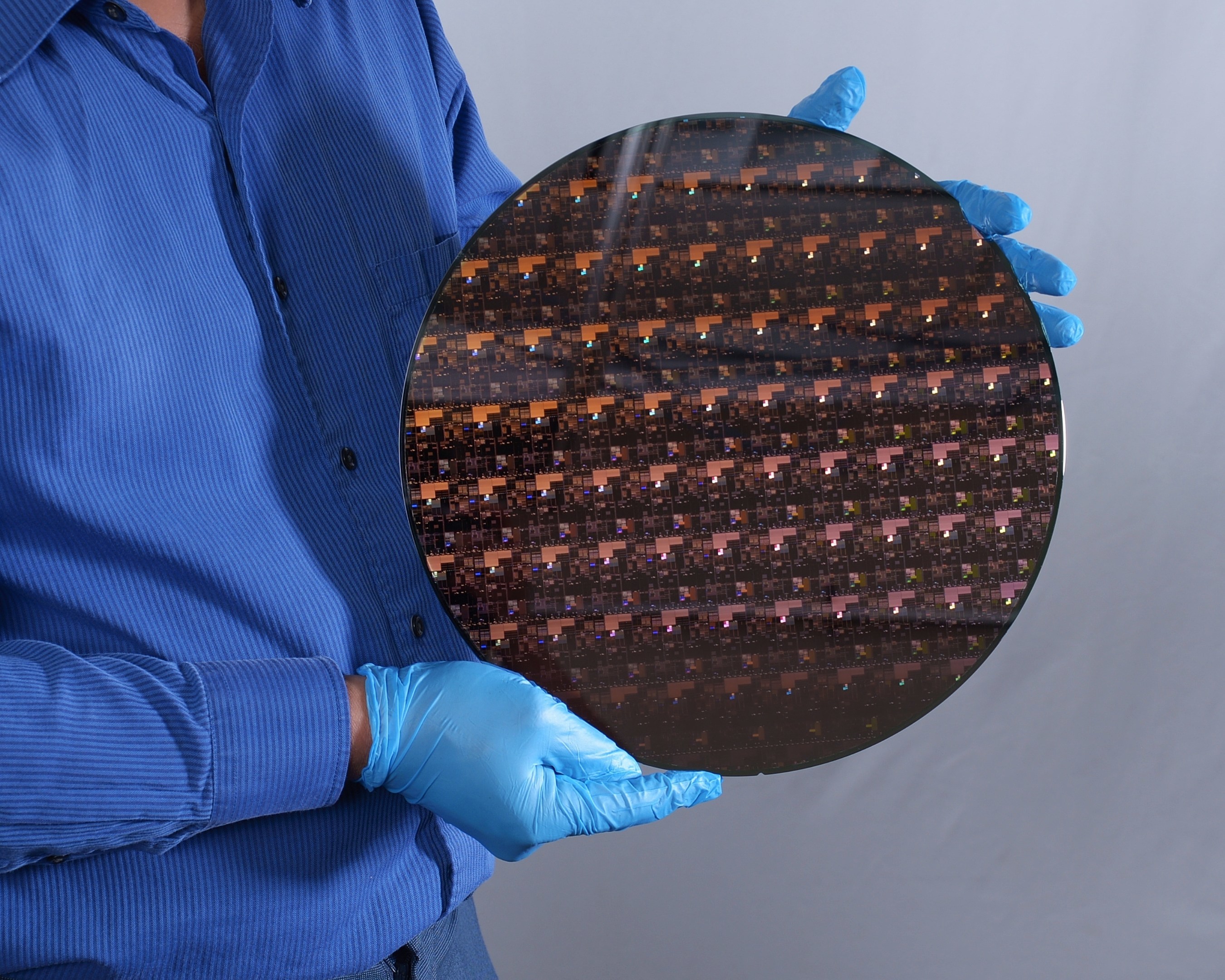
Samsung announces 2nm manufacturing process with GAAFET transistor technology
Samsung’s semiconductor production has been a center of negative news lately. Apart form delays, Samsung processes are believed to be inferior to TSMC node-for-node. But despite this Samsung is still the number two in leading edge process nodes out of the Foundry producers. Now the company has announced 2nm node, which should go into production in four years, two to three years after the volume ramp of the 3nm technology.
Previous Samsung (public) roadmaps were ending with the 3nm technology. According to latest public statements, the 3nm 3GAE process production should begin next year (a delay from the originally planned year 2021 which has occurred partially due to the coronavirus pandemic besides other reasons).
However it’s still possible this is a situation where the 3GAE (3nm GAAFET Early) process might not be broadly utilised, being relegated to status of more or less trial technology that will only be productised in some Exynos chips. That’s because Samsung could manage with worse yields or parameters (like clocks or energy efficiency) in their own products, that an external customer would not accept.
This possibility was being hinted at by roadmaps shown by Samsung this summer that did not display 3GAE and only featured the second generation of the process, 3GAP (3nm GAAFET Plus), which will arrive in 2023. On the other hand, Samsung now claims that the 3GAA process will be ready for customer sale in the year 2022, as well, contrary to the belief that 3GAE might end up being for internal and test use only. It remains to be seen how this plays out.
2nm process node
In any case, Samsung has presently confirmed that it does not intend to end on the 3nm level and plans on further continuing in the leading-edge silicon lithography race with the 2nm technology. This has not been featured in the previous roadmap (although the research and development surely have already been in progress) and it is only now that it is being officially added to it.
However this technology is currently still a matter of the relatively distant future. Samsung states that that production with this technology will start in the second half of the year, this would be two or three years after the start of the 3nm process – depending on whether it will actually start in 2022 (in the 3GAE form) or in 2023 (3GAP). However the second half of the year 2025 should already mark the beginning of a full scale volume production of product chips, not only the testing „risk production“.
Unfortunately Samsung does not share any parameters of the 2nm process yet. We therefore do not have a clear idea on how much will the transistor density and energy efficiency improve and how it will compare with competing technologies – 4nm, 3nm and 20Å processes by Intel and 3nm and 2nm processes by TSMC.
More: The first 2nm chip has been made by IBM Research
Smooth 2nm introduction thanks to 3nm node trailblazing?
According to Samsung the introduction of the 2nm technology should be relatively smooth without any major issues. It can be objected that it is all too easy to promise something like this four years in advance, but the statement has a certain factual base. The 2nm technology is not a particular breakthrough being rather an evolution of sorts. Samsung is preparing for the deployment of a new transistor type, the so called GAAFET (also known as MBCFET) using nanosheets, during the 3nm generation. The GAAFET will be the actual major change and problems are to be expected with its introduction. Samsung will need to solve those already during the deployment of the 3nm process, which might suffer in terms of quality, or run into delays – as we might have already experienced since it is delayed.
But it might be presumed that two years later during the start of the 2nm process the GAAFETs will already be under control, exactly thanks to the previous perils experienced during the 3nm generation, and thus the greatest challenge should already be conquered. Only much less demanding incremental improvements and tuning will be needed after that, which should be comparatively much easier. It is therefore indeed rather likely that the 2nm process could ramp up with less difficulties than the 3nm.
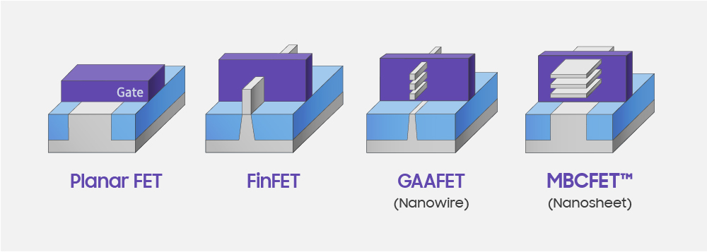
In this context we should mention that competitor TSMC intends to deploy GAAFETs only with the launch of their own 2nm process, while still relying on last-gen FinFET transistor structure for the 3nm node. This likely enables TSMC’s 3nm technology to be offered earlier and with less difficulty, but this in turn will make the deployment of the new transistors more challenging since TSMC will be doing the initial volume deployment on a bit smaller and overall more difficult lithography. This could be an opportunity for Samsung to gain a better competitive positioning against their bigger competition form Tchaj Wan. Nevertheless TSMC expects to launch their 2nm process already in the year 2024 and it is therefore possible that it might outpace Samsung and again leave it behind, despite the mentioned risks.
Even Intel has scheduled their 20ångström (2nm) process for 2024, and therefore it might jump ahead of Samsung as well. That however is assuming that the actual xecution won’t fall behind delaying the schedule. Intel will only be deploying GAAFETs (though it calls them RibbonFETs) with the launch of their 2nm technology as well just like TSMC, so they might also expect the introduction to be a greater challenge (but that in turn making 3nm process easier).
Sources: Samsung, Tom’s Hardware
English translation and edit by Karol Démuth, original text by Jan Olšan, editor for Cnews.cz
⠀