Big and „small“ cores: what are the reasons?
Intel has revealed the Alder Lake CPU architecture, or actually two architectures this time. The CPUs are hybrid and besides the main „big“ ones, there are „little“ cores called Gracemont. These are not just for marketing or for low-power idle tasks like in mobile ARM SoCs, however. Gracemont should significantly add to the overall performance, the architecture is actually surprisingly beefy. Our analysis will show you more.
The so-called „big.LITTLE“ scheme has been subject to much criticism or at least scepticism ever since the first news suggesting Alder Lake is going to be like this surfaced. There are prevalent opinions that it will hold the processors back, at least in the desktop PC segment, if not everywhere else too. We have to wait for independent reviews upon launch (or perhaps even a bit further than that) to actually get definitive answers to this question, but even the on-paper characteristics of the Gracemont core microarchitecture are quite a significant sign that things won’t quite go the way detractors have generally expected. One thing particularly stands out: the whole debate might have been thrown off the right track from the start by the use of the „little core“ naming. Because it seems that Gracemont doesn’t quite fit the concept of a little core and it’s not a good way to call it. Unsurprisingly, this itself might be a large contributor to our expectations being off.
Indeed, Intel doesn’t call Gracemont „little core“ (that is actually 100% unofficial parlance) and instead uses the term „Efficient Core“ (E-Core), meaning a core that has high efficiency—which should refer to energy efficiency and also silicon area efficiency. It might be beneficial if we just dropped all our preconception and notions of big.LITTLE for now and even ignored Gracemont’s lineage, derived from the past Intel little cores that have been bearing the Atom brand, for a moment.
Based on what Intel has presented about Alder Lake, its hybrid architecture using two types of cores is actually envisioned as a solution to a problem that is not actually something stemming from the mobile area, but a more general problem of optimal sizing of processor cores for various different types of software tasks—an issue that is very relevant to desktop processors. This might mean that any mobile area benefits Alder Lake brigns, like longer battery life, could even be merely secondary benefits rather than the primary goals of this architectural decision.
Solution to dilemma between best ST or best MT performance?
What is actually this problem we mentioned? It’s like this: there are various demands we put on a high performance processor. One of the most important ones is performance while executing a single thread, a.k.a. single-thread (ST) performance. This ability is crucial for many different desktop and notebook tasks, but it also contributes to performance in games and to responsiveness of operating system’s GUI, apps, pages open in web browsers and so on. However, this performance characteristic is not the only one. Besides it, there is also the similarly very important multi-threaded (MT) performance—the amount of performance the processor is able to provide for programs that are able to utilise all its cores and threads simultaneously. Multi-thread tasks tend to be very heavy and often can be long running, which means that any performance boost can lead to appreciable savings in your time, which single-thread performance, while possibly improving your experience and comfort, might actually not. The whole issue is that it just so happens that a processor core designed to maximally excel in the first single-thread metric can very easily end up not being optimal for the second, multi-thread performance metric. When you design your cores to be best in ST, you might end up harming your MT ability, and vice versa, optimising for MT might result in cores weaker in ST performance.
On a side note, this dilemma has been explicitly acknowledged by ARM, which actually does try to solve it in its portfolio of CPU cores by providing two different designs for each task, into which the company has split its previously unified big core design. After Cortex-A77, the company started to provide a more efficient Cortex-A78 and now A710 core microarchitectures that are more MT-optimal, and on the other hand heavier Cortex-X1 and X2 cores that prioritize ST performance at the cost of MT performance ability.
For a core targeting maximum single-thread performance, it makes sense to make many compromises that trade in relatively large jumps in transistor count, complexity and power usage for relatively smaller gains in overall performance. For these cores, it could be perfectly reasonable to accept a +30% power consumption and silicon area hit to gain an extra +10% performance increase. This is because single-thread performance is highly coveted and also, a program running just on a single thread does not hit TDP limits for the whole CPU in most processors (it actually might do that in sub-15W chips and in ~5W phone SoCs, though).

However, when you want to maximise multi-thread performance, you will often see that the ST trade-offs hurt you. Multi-threaded performance is usually bound by the power consumption it is allowed to reach (TDP). The architects basically have to reach the best MT performance (which means the best possible combined performance across all cores/threads simultaneously running) they can within the envelope of a limited wattage. But this is not compatible with spending 30% more power for +10% per-core performance, because that would actually lower the performance you get per watt. For maximising MT performance, you need solutions that scale performance in balance with power and actually bring more extra performance than what they cost in power. A good strategy might be running your cores at lower clock and thanks to that at lower voltage than what you would run them at for ST tasks—because that increases efficiency (performance per watt)—and compensating by making use of more of these cores. However, to be able to increase the number of cores, you might be forced to cut-down their silicon area footprint (number of transistors), because extra chip size costs money and you inevitably run into your silicon budget limits (and related constraints your management will put on your design’s manufacturing costs).
Due to these factors, the best design of core for purposes of achieving MT performance is such an architecture that doesn’t actually shoot for maximum single thread performance and is more relaxed about it: for example a core that sacrifices the last 10% of possible single-thread performance, but in return is able to reduce the power consumption and silicon area footprint by 30%. With that, such cores can, given a certain count of them in the chip, achieve a higher overall multi-threading performance in the envelope of a particular TDP budget they are given (be it 35W, 65W or 125W).
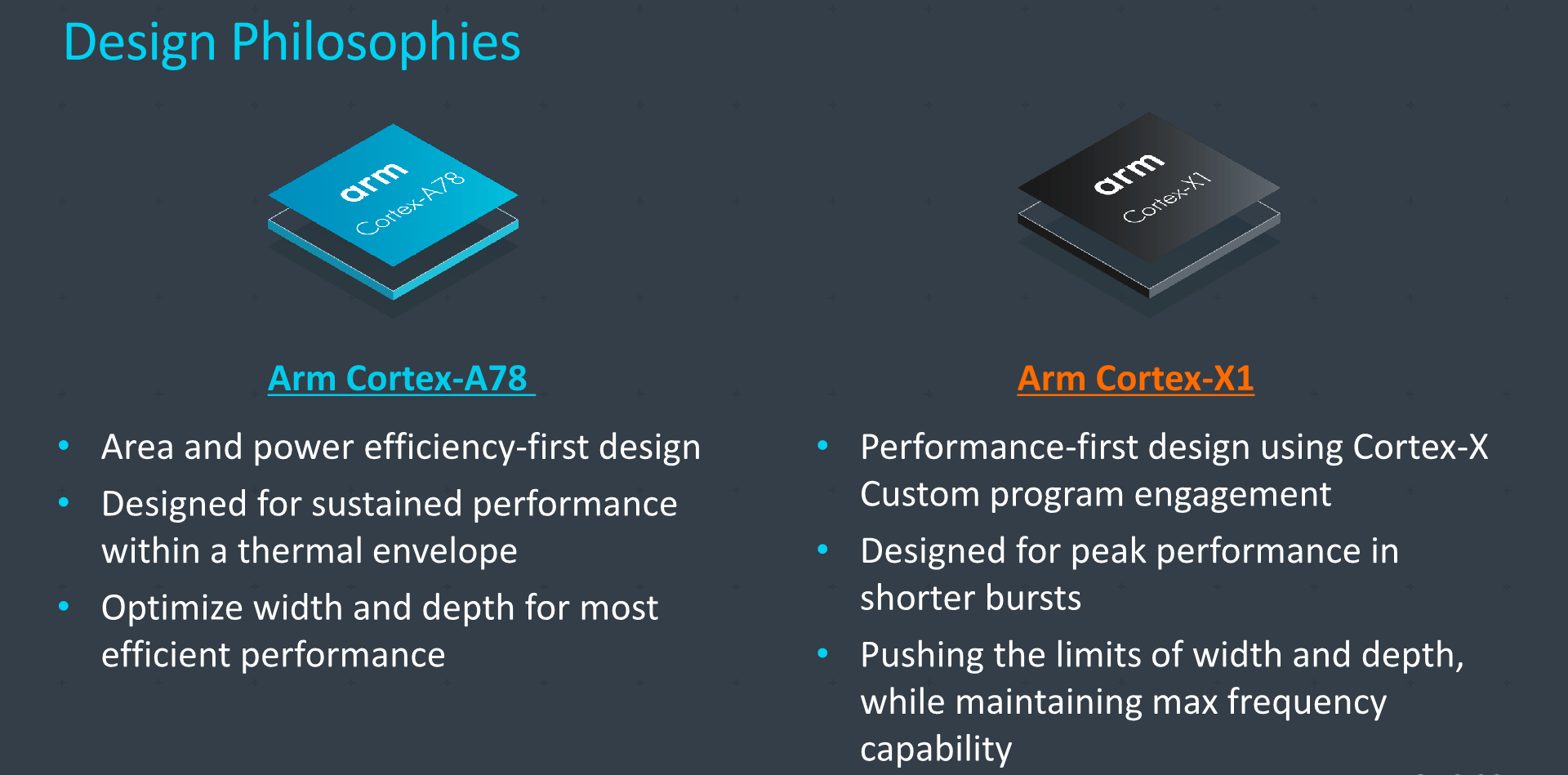
In the case of ARM processors, this latter strategy is what governs the design of the Cortex-A78 or the current new A710, cores designed to be power and area optimal, while still belonging in the category of big cores. Thes first strategy that maximises ST-performance at the cost of worse energy efficiency and suboptimal core footprint in the chip has produced the Cortex-X1 and X2 cores.
It seems that in the case of Alder Lake, the Golden Cove can be likened to the Cortex-X line, and precisely like in the case of Cortex-A78 or A710, the Gracemont core is not really a little core, but at least a “medium”, if not a “smaller big” core. Intel’s choice to call the cores Performance Core and Efficiency Core instead of the big and little terminology reflects this, too.
The actual goal of the hybrid architecture then is to do away with the described dilemma and to not have to pick whether the processor will use cores that are ST-friendly or cores that are more MT-friendly due to being smaller and more efficient.
With its hybrid combination of cores, Alder Lake and its successors have the advantage that they can mostly do both at once. The processor will contain a certain number of the big performance cores that are optimised for maximum single-thread performance to cover the need for that for single-thread tasks. However, it will be just this limited number of cores that will have to bear the efficiency hit, because the rest of the cores will use smaller efficient microarchitecture that is optimised for multi-thread performance (this is also called “throughput” sometimes, or “scalability”). The addition of these cores improves the combined MT performance of the processor achievable within a given TDP limit, but also within a certain die size limit. The ST performance is not needed to be the very best on all of the cores but merely on a few that will be used for the relevant tasks and for games—as long as the operating system is clever enough to schedule such programs to the right cores. It might therefore be advantageous to actually use the little (or rather, efficient) architecture for most of the cores in the processor. It seems this actually might be exactly what Intel is planning. While Alder Lake uses an 8+8 combination, the leaked rumors suggest that future generations will shift the balance towards a much bigger share of efficient cores: we might see CPUs with 8 performance and 16 or later even 32 efficient cores.
Theory is nice, trial by fire is yet to come though
The reason we subjected you to this lengthy preface was to explain that there are some sound theoretical arguments to be made in favor of hybrid („big.LITTLE“) strategy, and they might hold true even for desktop high-performance processors. Even despite the prevalent scepticism that it is readily seen everywhere, including your comments under our articles that show that large part of hardware enthusiasts doesn’t expect this idea to be successful in PC processors and have negative expectations.
To be clear: we don’t yet know for sure if Alder Lake actually does manage to successfully solve the problem we just described. Sometimes even sound and well-researched ideas might fail to transform into a working solution. There are possible pitfalls, for example Intel might fail to make their implementation of efficient cores efficient enough to outweigh possible scheduling problems an asymmetric processor could cause. The concept behind the hybrid decision does seem reasonable and viable though.
With that said, let’s finally get to the promised analysis of the Gracemont microarchitecture itself. We however recommend that you read the similar analysis of the big core, Golden Cove (Performance Core), first, in case you have not done so yet. The little Gracemont microarchitecture (Efficient Core) should be viewed in context of its larger sibling architecture.
Suggestred reading: Intel Alder Lake/Golden Cove CPU core unveiled (µarch analysis)
The article continues in the next chapter.
- Contents
- Big and „small“ cores: what are the reasons?
- Gracemont: the „little“(?) microarchitecture has reached Skylake levels of performance
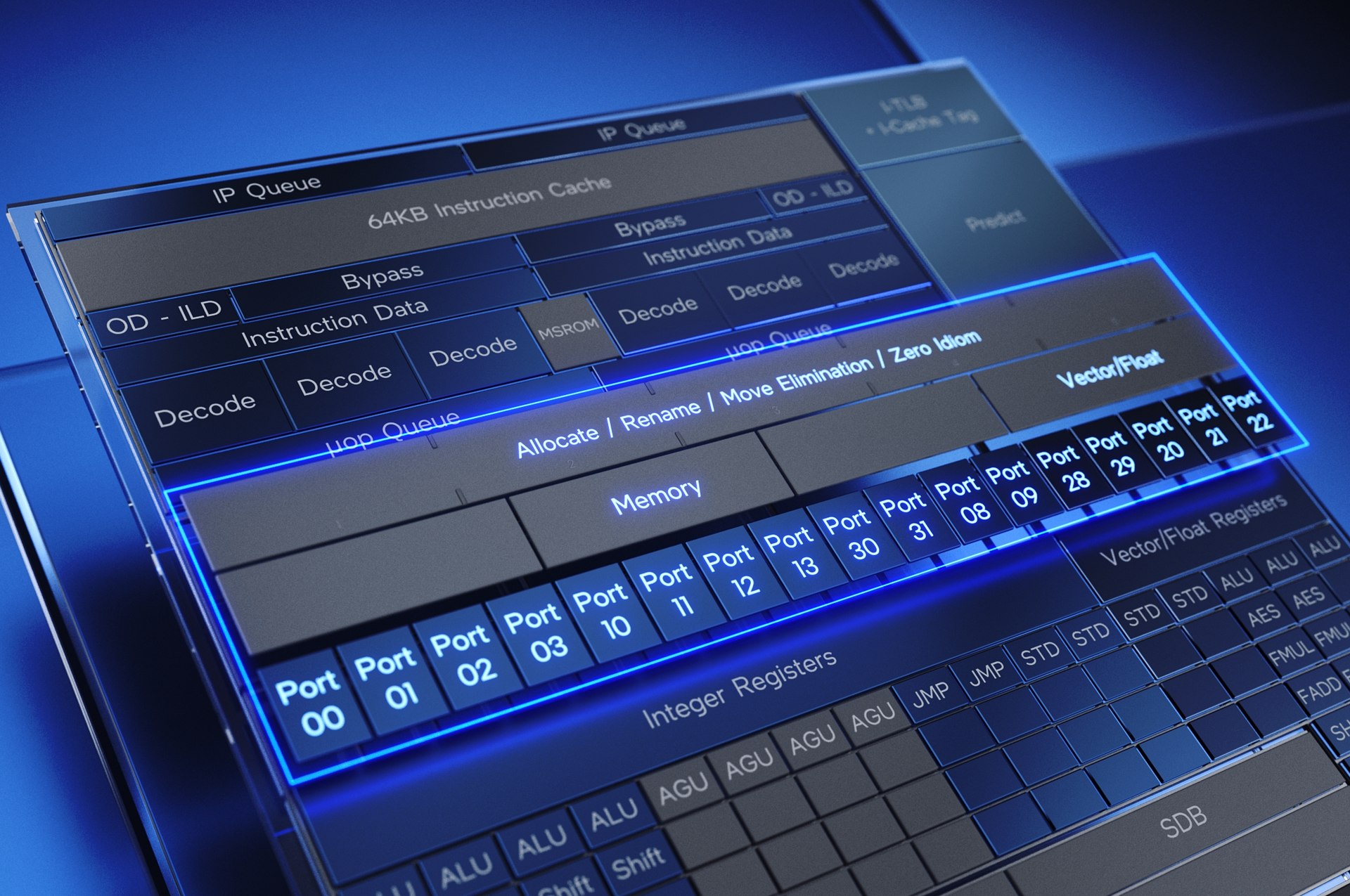
- Execution units: 17 ports and high IPC potential
- Memory subsystem: AGU and Load/Store resources doubled
- Speed: „Little“ core’s performance is up to two thirds of a big one