Memory subsystem: AGU and Load/Store resources doubled
Intel has revealed the Alder Lake CPU architecture, or actually two architectures this time. The CPUs are hybrid and besides the main „big“ ones, there are „little“ cores called Gracemont. These are not just for marketing or for low-power idle tasks like in mobile ARM SoCs, however. Gracemont should significantly add to the overall performance, the architecture is actually surprisingly beefy. Our analysis will show you more.
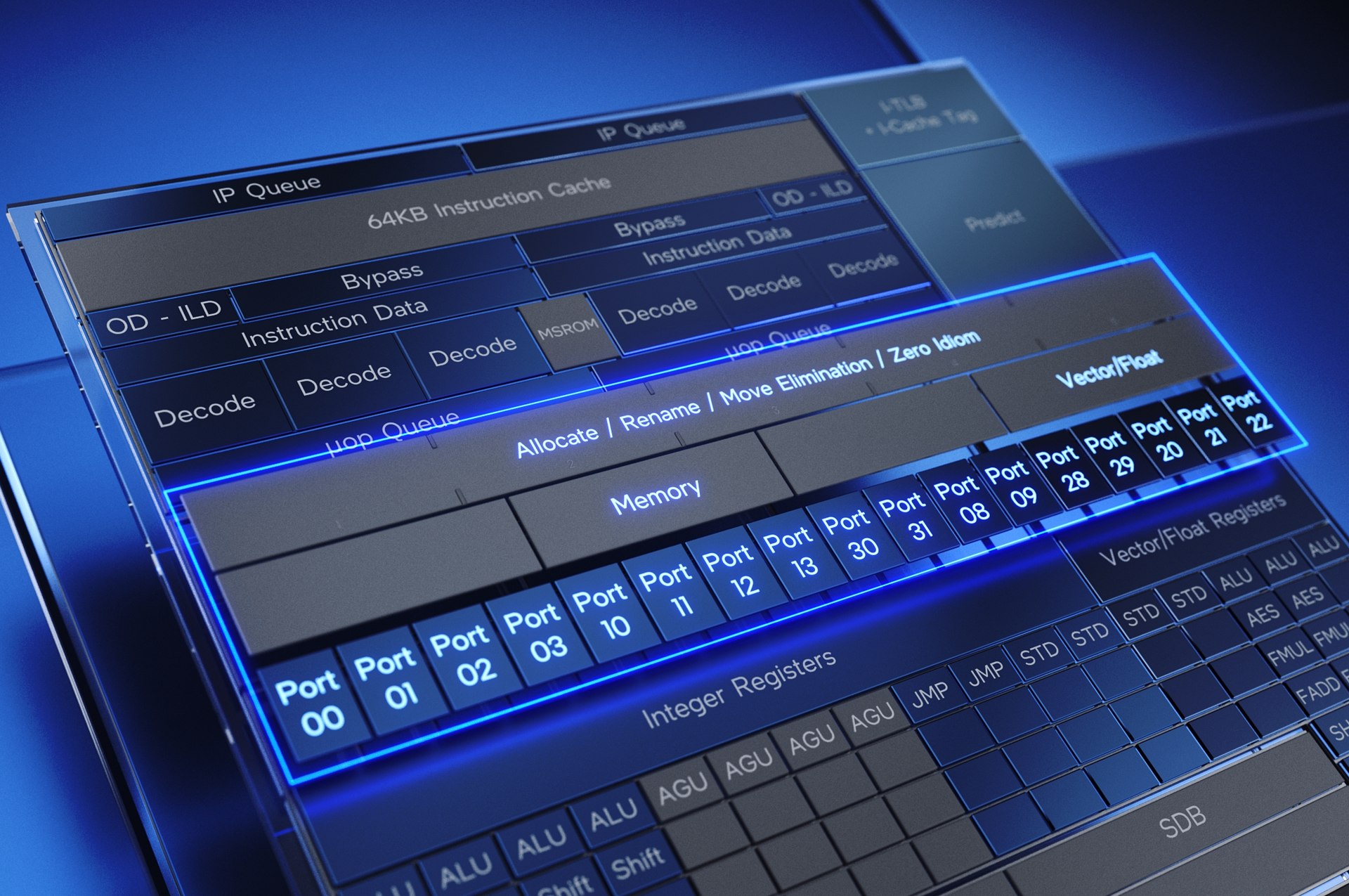
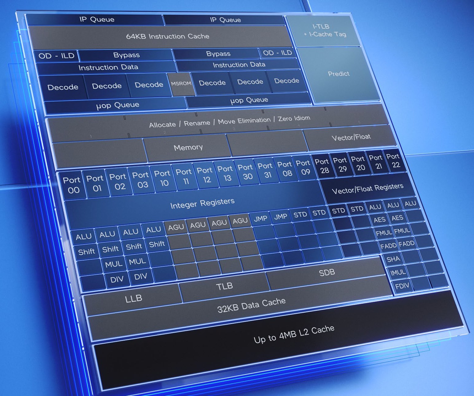
The Load/Store part of Gracemont core is another very strong story: the core has four AGUs (address-generation units) on ports 10, 11, 12 and 13 and their pipelines can perform two reads and simultaneously two writes to the memory (or to be precise, towards the L1 data cache). This Load/Store capability matches the big Ice Lake/Tiger Lake/Rocket Lake processor cores, so we can consider the Load/Store subsystem very powerful. Tremont core had just two AGUs that could do only two memory operations per cycle in total, two reads or two writes (or 1+1 mix). The width of the memory operations is 16 bytes (128 bits), which means the core can read or write the data of two 128-bit SSE* vectors or one 256-bit AVX(2) vector per cycle—32B per cycle.
Gracemont is worse than the very strong Golden Cove in the bandwidth achieved. Golden Cove can’t do that many more operations (3 loads + 2 writes per cycle), but it crucially uses paths that are double the width, 256 bits (32B). This gives it significantly better bandwidth with reads theoretically possible at 96B/cycle and writes at 64B/s. This could cause huge differences in demanding SIMD computations using lots of data. On the other hand, for example Zen 3 provides nowhere near this bandwidth (it’s mostly half Golden Cove’s width and bandwidth, but also has just three AGUs instead of five). Yet its overall good performance shows that this could be less of a handicap than one would assume, or at least that it does not become a severe bottleneck that often.
The difference that Gracemont uses two dedicated Load pipelines and two dedicated Store pipelines while Tremont used two universal Load/Store pipelines means that when program code simultaneously reads and also writes data from cache, Gracemont can reach up to 2× throughput of these memory operations, so a significant theoretical bottleneck has been alleviated. However, in the case of code that largely just reads or just writes at a time and doesn’t mix the two, there is no difference compared to Tremont.
Lastly, similarly to Golden Cove, Gracemont also uses two separate pipelines on their own dedicated ports (8,9) for Store Data.
Cache: shared L2 (and L3)
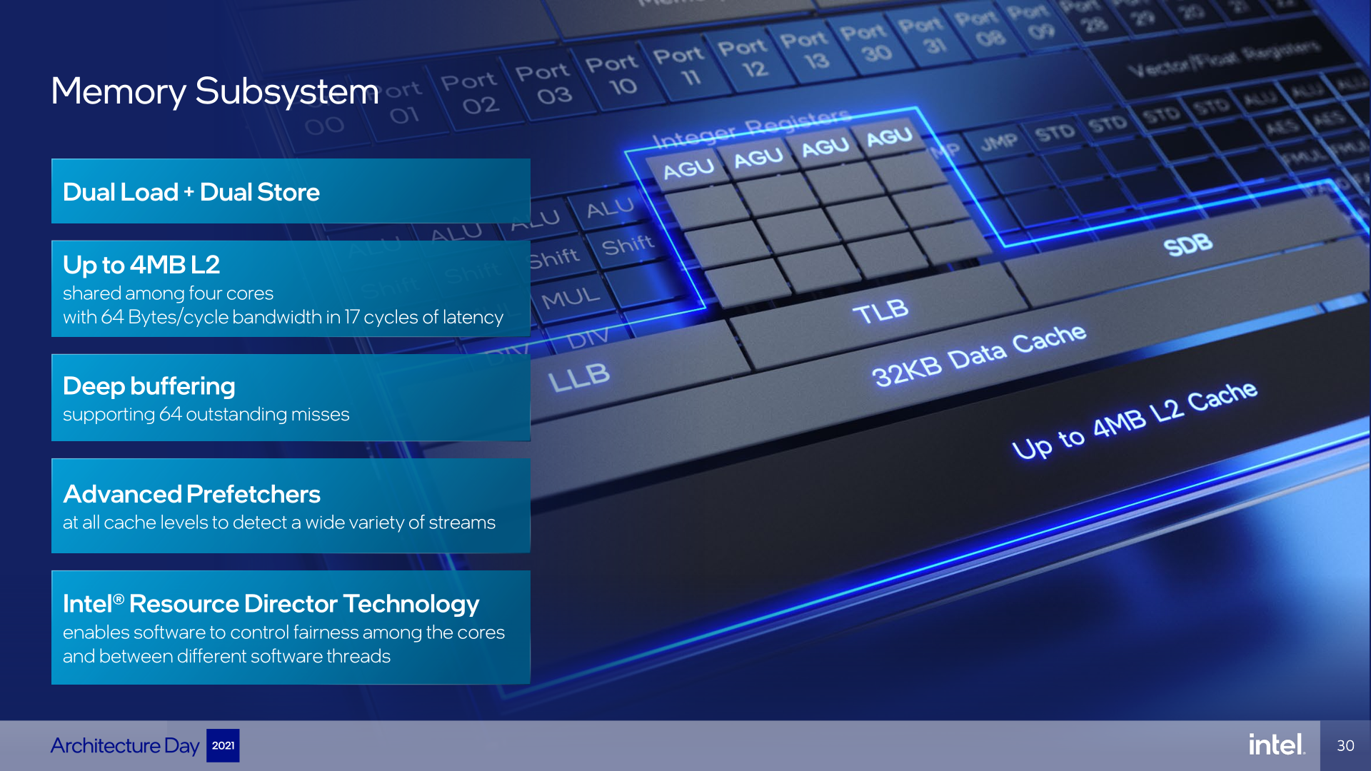
The L1 data cache of Gracemont has a capacity of 32 KB, which is smaller than the 48KB L1D serving Golden Cove (Sunny/Willow/Cypress Cove in Ice/Tiger/Rocket Lake processors). It is however as big as also 32KB sized L1D of AMD’s Zen 3 core. In the case of Gracemont, the 32KB cache might however be lower-latency. Intel doesn’t state the overall latency, however it mentions that pointer-chasing is only 3-cycle latency (it is possible that other, general-case operations are 4-cycle latency).
L2 Cache has configurable capacity in Gracemont. it can be either 2MB or 4MB. This however is not per single core, instead the L2 cache is shared between a cluster of four Gracemont cores that forms a basic building block of this architecture. Based on information that has leaked some time ago the implementation in Alder Lake only uses the lower capacity, meaning that the quad-Gracemont clusters in the processors will each have just 2MB of L2 cache.
The bandwidth of this cache is 64 bytes per cycle (1024 bits/cycle), which is a decent amount of bandwidth for four cores. The latency is 17 cycles according to Intel which would be bad for a small dedicated L2 cache but we suppose it is acceptable for this large cache shared by four cores. Gracemont’s L2 Cache supports up to 64 parallel outstanding cache misses (these are requests for data that have not been found in L2 cache and thus are being requested from L3 Cache or RAM). Ability to have a large number of outstanding cache misses in flight improves memory performance. Bigger buffer of these operations decreases the chance that the core has to wait with further data requests because the earlier misses have not yet been served.
Intel says prefetching has been improved for all cache levels in Gracemont and the prefetchers are able to detect many more access patterns and select proper prefetch strides for them. Gracemont also supports Intel Resource Director technology, which allows software to configure bandwidth allocations and QoS for individual cores/threads.
Whereas L1 cache and L2 cache are part of Gracemont microarchitecture, we won’t directly cover the L3 cache here as Intel has not talked about it in the architectural reveal. Based on what we do know so far from unofficial sources, L3 cache will be common (and shared) to both Golden Cove and Gracemont cores in Alder Lake and the cache parameters will therefore be the same for both, Intel’s L3 cache is tied to the ring bus interconnect that will be connecting the big and little cores together. Or to be more precise, we should say it will connect big cores and clusters of little cores, because it looks not the individual Gracemont cores, but the whole quadcore cluster will be the client of the ring bus. In line with that, the quadcore cluster of course also has just one shared block of L3 cache, which should be identical to the same block that a single big Golden Cove core will have. The capacity of this block should be 3 MB in Alder Lake. The top SKU with 8 big and 8 little cores should therefore have a 30MB L3 cache comprised of 10× 3MB.
The article continues in the next chapter.
- Contents
- Big and „small“ cores: what are the reasons?
- Gracemont: the „little“(?) microarchitecture has reached Skylake levels of performance
- Execution units: 17 ports and high IPC potential
- Memory subsystem: AGU and Load/Store resources doubled
- Speed: „Little“ core’s performance is up to two thirds of a big one