

Gracemont: the „little“(?) microarchitecture has reached Skylake levels of performance
Intel has revealed the Alder Lake CPU architecture, or actually two architectures this time. The CPUs are hybrid and besides the main „big“ ones, there are „little“ cores called Gracemont. These are not just for marketing or for low-power idle tasks like in mobile ARM SoCs, however. Gracemont should significantly add to the overall performance, the architecture is actually surprisingly beefy. Our analysis will show you more.
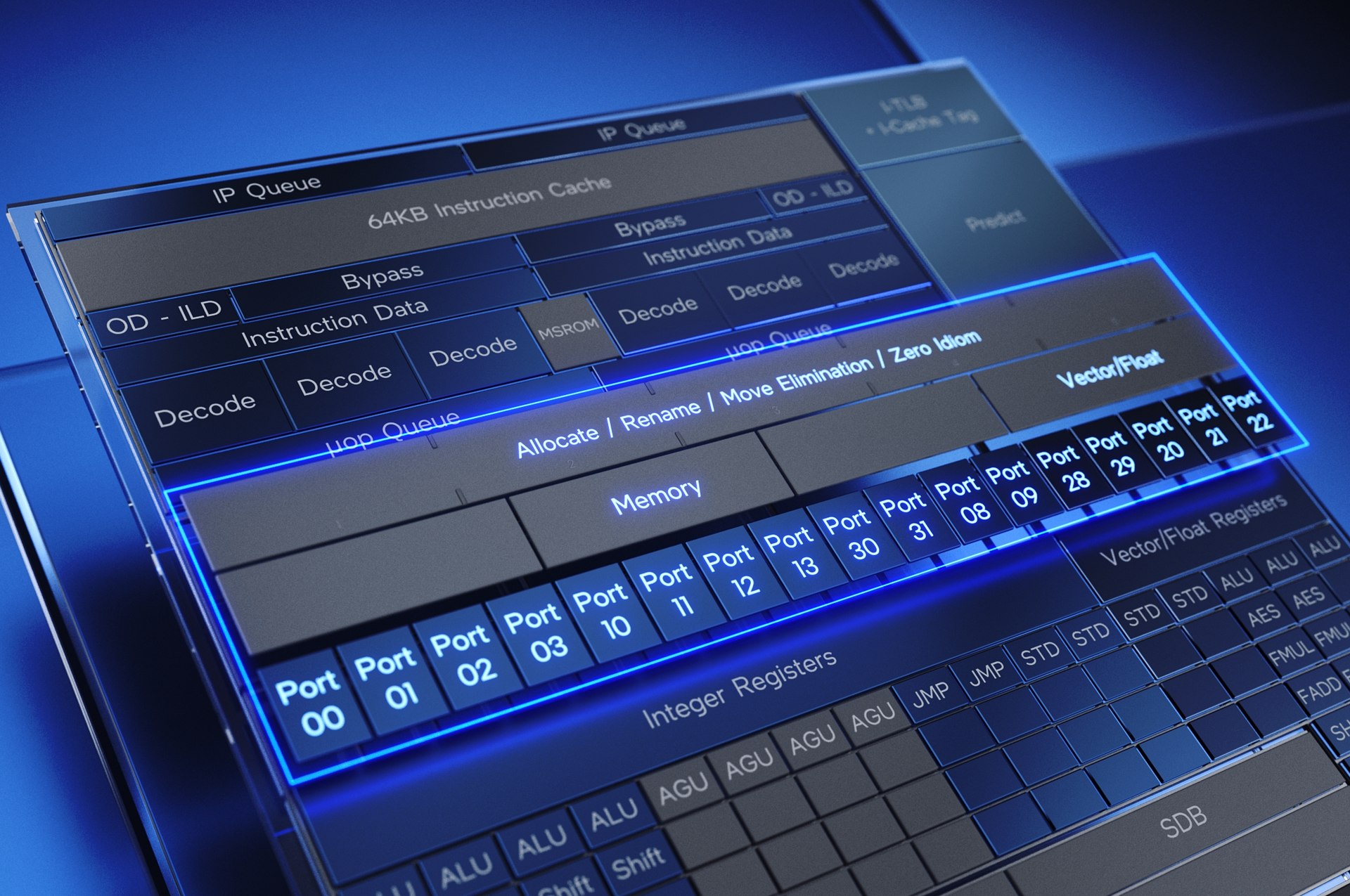
The goal of Gracemont was to design a core that achieves as high performance as possible within as little silicon footprint (and power consumption) as possible, which would allow good multi-thread performance scaling by adding more of these cores. The performance of the core should be around or even above the level of the older Skylake core—at least when looking at the same clock frequencies—but with Gracemont consuming much less power.
With IPC that is higher than Skylake, the core was also to be designed to run at low voltages, that would allow it to reach power consumption that is a fraction of what Skylake runs at. Intel even claims that Gracemont is the most power-efficient x86 core in the world to this date (meaning that it has the best power/performance ratio in the world).
There is one crucial difference: Gracemont is simpler in the aspect that it always executes just one thread, there is no form of HT (SMT) capability. We don’t know if Intel is absolutely opposed to adding this feature to Efficient Cores meant for this purpose, for example due to the costs that would pose in complexity, power draw and the extra transistors needed. It could be that the company doesn’t actually rule out Efficient cores with HT and it just didn’t get around to adding it to this architectural lineage yet. HT is a feature that has natural synergy with wide higher-performance CPU cores and Gracemont is actually a surprisingly wide design.
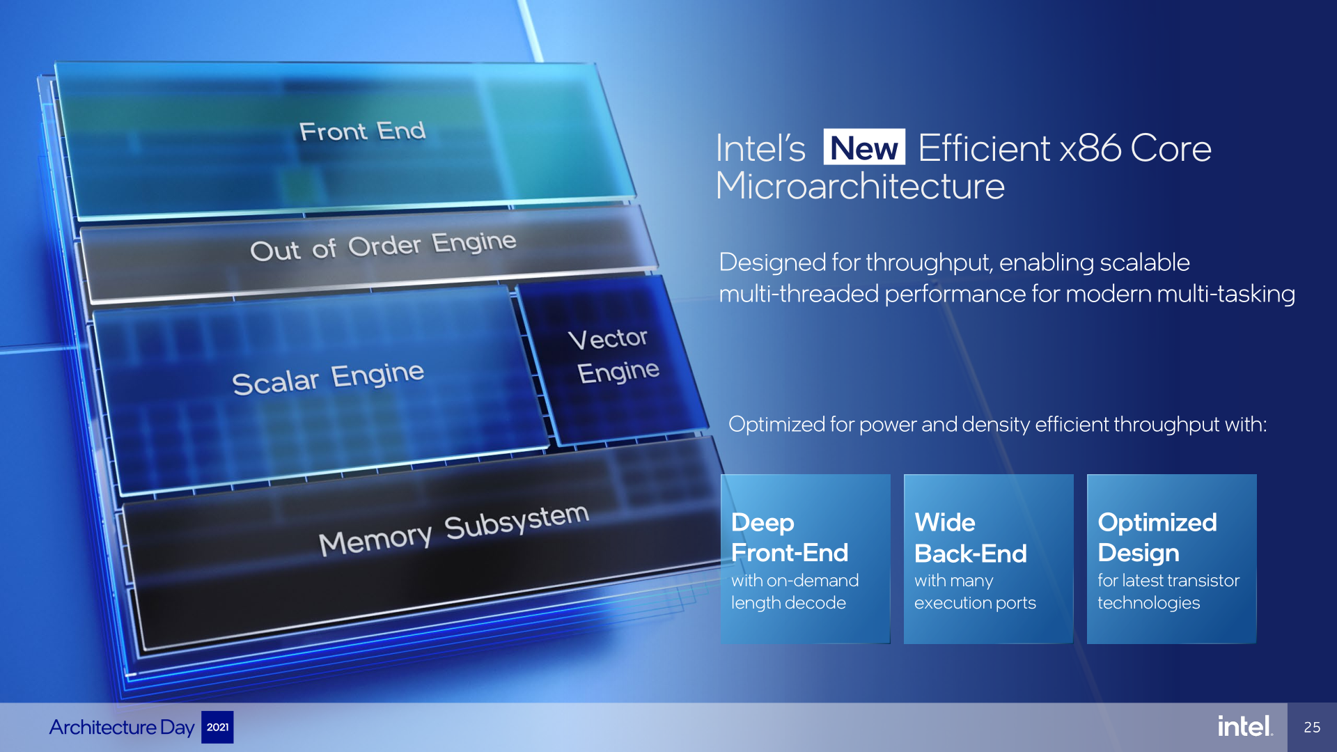
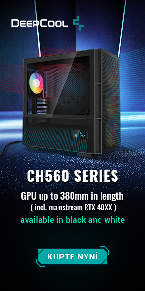
Frontend with 2×3 decoder clusters
Gracemont’s design does show that it has evolved from the past members of the Atom family of cores, but the architecture has been substantially beefed-up (widened and deepened). The core inherits the most striking feature of the previous Tremont architecture: its dual-cluster instruction decoders. Gracemont, like Tremont before, uses two clusters of decoders, each comprising of three units. The combination of these two clusters isn’t as strong as the six-wide decoder setup (which is a single cluster) in Golden Cove. The clusters can’t always couple up together to decode six consecutive instructions per cycle. What they can do is parallelly decode two instruction streams, with three decoded instructions per cycle in each of the streams. This solution is more energy and area efficient than the strong 6-wide decoding of Golden Cove.

The two clusters can be used simultaneously in some cases, for example when the processor knows there is a jump due to branching. It can then use the jump’s target address as a starting point from where the second instruction stream can be fetched and decoded on parallely using the second cluster. Branches can actually be quite common in code (Intel mentioned that they can commonly happen as often as every 6 instructions in the program), which means that even this at first sight limited usability of the second decoder cluster can matter surprisingly often.
While the decoding capacity is the same as in Tremont, the L1 instruction cache of the core has been doubled from 32KB to 64KB (which is 2× more than Golden Cove has, by the way). Similarly, Branch Target Cache used by the branch predictor has been enlarged and has capacity of 5000 entries in Gracemont (but we do not know that this value has been in Tremont). This should enhance branch prediction accuracy. The predictor also works with a long history, which should again improve its success rate.
Predecode stores meta information into L1i cache
The core uses an optimisation called On-Demand Instruction Length Decode. What it boils down to is that the processor does a predecode work when it loads parts of program code into the L1 instructions cache, and this predecode determines lengths of instructions in the code, which is then stored in the L1i cache as metadata. This gives the core an idea where individual instructions begin and the knowledge is reused when the processor reruns the same code (for example in loops), since part of the energy-intensive decoding work can be skipped.
Tremont has no μOP cache that would store fully decoded instructions for later reuse, like the big Golden Cove core (Intel uses μOP cache since Sandy Bridge, AMD since Zen 1, and even ARM with its fixed-length instruction set does, since Cortex-A77). One of the motivations besides performance is that μOP cache lowers power consumption. Using predecode and remembering the instruction boundaries seems to be an alternative to using full-blown μOP cache, an alternative that is simpler to implement and much cheaper in transistors needed (and hence requiring much less silicon area footprint). But also on the other hand an alternative that is less advanced.
Beefing-up the out-of-order engine and execution units
The biggest upgrades and strengthening changes Intel has done to the Golden Cove core were in the frontend, while the backend of the core (the execution units themselves) were boosted comparatively less. However, the Gracemont core is almost the opposite. While its frontend is not so different from Tremont, the core’s execution unit backend was widened and strengthened significantly. There is one thing common with how Intel evolved Golden Cove though: improving the middle-stages of the core, where the out-of-order optimization and reordering of instructions to be executed happens.
The Allocation stage in Gracemont can process up to 5 instructions (or better said, μOPs) coming from the decode stage and the μOP queue, per cycle. This capability is 25% better than in Tremont which was 4-wide for this stage. Gracemont also doesn’t fall much behind Golden Cove, which has 6-wide Allocation (6 μOPs per cycle). What this stage performs is allocating their working registers to individual μOPs. Also handled here is renaming registers to hide conflicts that happen in the code due to reusing the same limited number of architectural registers. Internally renaming (substituting) the registers allows such nominally (but not actually) conflicting operations to be performed simultaneously gaining performance. The processor also can eliminate some operations that don’t actually have to be scheduled into execution units altogether, in this stage (MOV Elimination, handling zeroing idioms).
Out-Of-Order window as big as Zen 3 has
Following this, the pipeline continues with the Re-Order Buffer (ROB), which is a queue that the processor can use to reorder the instructions and to pick those that are to be executed next, ideally achieving as much work being done in a single cycle as possible, utilising as many of the available execution units as it can. Out-of-order CPU can execute operations that do not depend on each other in parallel and if it happens that the instructions that are supposed to enter execution don’t yet have their prerequisites ready (due to data dependency, dependency on result from preceding instruction), it can reach further into the future to execute other independent instructions instead. This compacts-down the code so that it is fully executed within fewer cycles in total. However, for these out-of-order optimizations to be effective, there is one important factor: the amount of instructions of the code (a.k.a. out-of-order window) the CPU “sees” for this purpose—the more, the better. This “window” is equal to the ROB queue in Intel’s processors, so to get best performance, we want a bigger ROB.
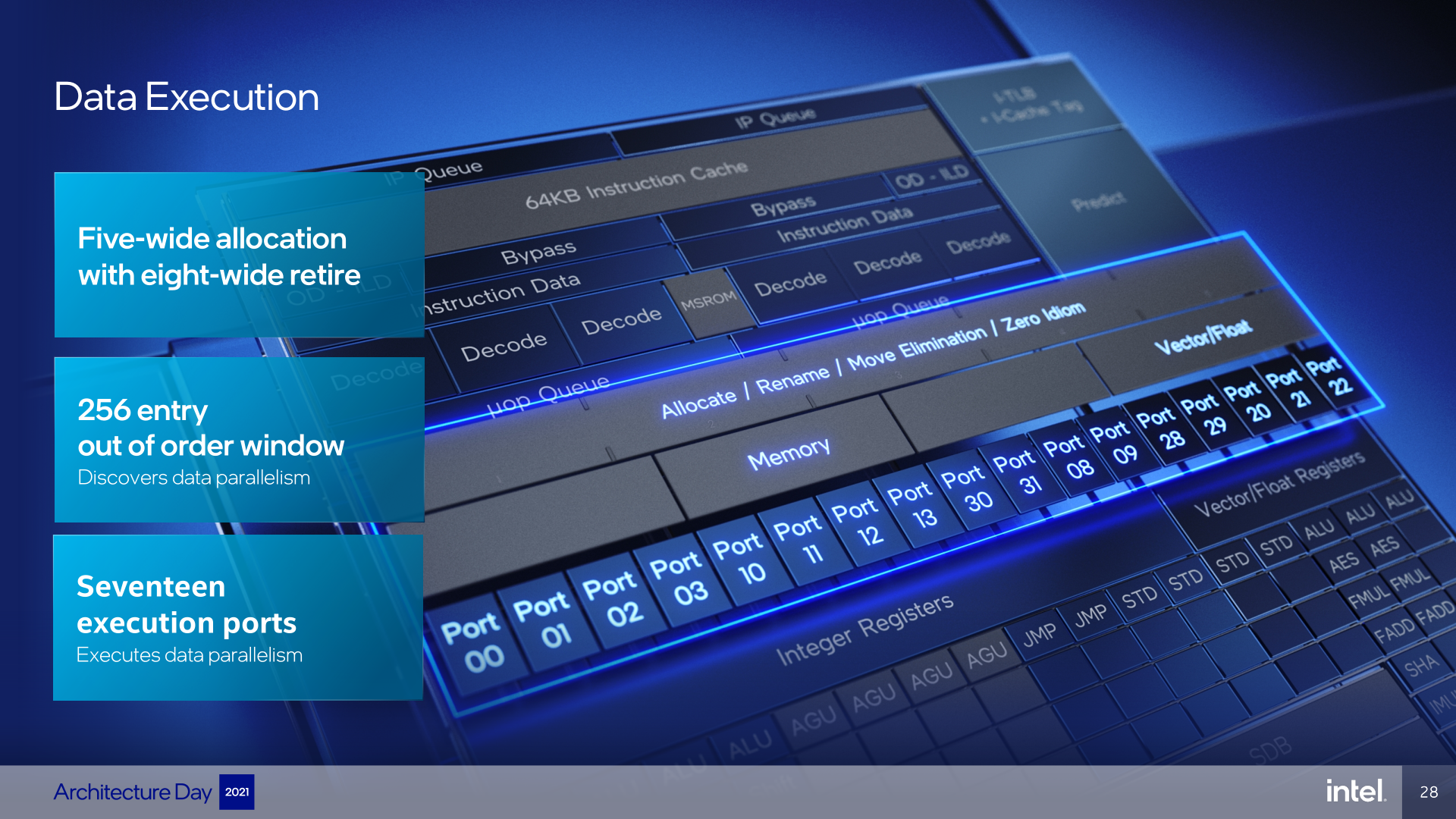
And the ROB (Re-Order Bufer) in Gracemont is relatively large, at least for a core that some would call little. It’s depth is 256 entries. This might be just half of what the big Golden Cove core has, but it is also more than the big Skylake core had (224). And what is notable, this value is exactly equal to the ROB size of AMD’s high-performance Zen 3 core. While it is likely that Zen 3 is somewhat of an exception with strangely small size and AMD will soon also boost ROB depth massively, this does show that Intel is relatively aggressive in its sizing in the Gracemont architecture, pushing outside of the “little core” realm.
The article continues in the next chapter.
- Contents
- Big and „small“ cores: what are the reasons?
- Gracemont: the „little“(?) microarchitecture has reached Skylake levels of performance
- Execution units: 17 ports and high IPC potential
- Memory subsystem: AGU and Load/Store resources doubled
- Speed: „Little“ core’s performance is up to two thirds of a big one