

GeForce now with Infinity Cache. RTX 4000 has a gigantic L2 cache
Recently we have reported on the specs of Nvidia Lovelace GPUs found in driver source code stolen and published by hackers. Another juicy bit has been discovered since then: the Lovelace architecture has a significantly larger cache memory. This will greatly increase performance with the same memory bandwidth. Nvidia is de facto preparing its own version of Infinity Cache introduced in AMD’s RDNA 2 GPU architecture.
The code bits found in the prepared drivers show that the GPU with the architecture codenamed Lovelace or perhaps just Ada (it seems that Nvidia tends towards this marking in some of the driver files), will have up to 96 MB “Nvinfinity” Cache, at max configuration. The function should be the same as with AMD, that means keeping a great portion of “hot” data (data processed by the GPU while rendering games) directly on the chip, thereby lowering the demand for memory access.
According to AMD experiments the 128 MB Infinity Cache causes a 512 GBps bandwidth GPU to perform as if it had double the bandwidth or even more. This kind of cache takes up a lot of space on the chip (that otherwise might have been used to fit more computing units), but it results in better power efficiency and performance. In some cases this design could even make the final GPU a bit cheaper in theory, since a narrower memory bus with a cheaper PCB and fewer memory modules can be used. The fact that Nvidia is about to utilize a similar solution likely proves that AMD had the right instinct on this one.
Whether this analogue/imitation by Nvidia will also get a special name similar to AMD’s Infinite Cache monicker, is currently unknown. According to the drivers it should be an enlarged L2 cache (AMD’s Infinity Cache is likely an L3 cache). Its larger L2 cache capacity will most likely be dependent on the memory controller width. At least in some of the GPUs, there should be 16 MB of this L2 cache per every 64 bits of the memory controller. This means that the AD102 high end chip with 18 432 shaders and a 384 bit memory bus will get 96 MB L2 cache. The Ampere architecture uses a 512KB block of L2 cache for every 32 bits of the controller (one channel), which only amounts to 6 MB in the high end GA102 GPU. So Lovelace/Ada cache will be a vast difference, even though the overall capacity will turn out lower than AMD’s highest-performance RDNA 2 architecture implementation (the Navi 21 chip includes 128 MB Infinity Cache).
Ada will have huge L2 @VideoCardz pic.twitter.com/sjMGXttX0Y
— XinoAssassin (@xinoassassin1) March 2, 2022
According to this math, further Ada/Lovelace architecture chips should have lower L2 cache capacity. AD103 with 10 752 shaders and 256 bit memory would have a 64 MB L2 cache and the AD104 (7680 shaders) with 192 bit memory would get 48 MB. Small AD106 and AD107 chips reportedly have a 128 bit bus and therefore should carry a 32 MB L2 cache – that is if Nvidia won’t for example opt to cut it in half, which is actually something done by AMD with its cheaper GPUs (Navi 23 and Navi 24). Eventually a big cache could be dropped in favor of a lower price – for example something that Nvidia could do is designing the cheaper chip of these two (L2 cache) without the large cache. However this is only a speculation. It is equally possible that Nvidia will maintain the same capacity configuration to memory channel ratio for all GPUs.
Ada/Lovelace architecture GPUs will be produced on TSMC’s 5nm process, which will provide them with a significant upgrade in power efficiency, when compared to the not quite ideal 8nm process by Samsung used in Ampere GPUs – this might be a leap corresponding to one and a half, or even two manufacturing process node generations. The 5nm process will simultaneously shrink the area needed for SRAM cells in the chip, which will lower the impact the large caches will inflict on the chips’ size and cost. The required die area should be much smaller, when compared to Infinity Cache in the current 7nm GPUs by AMD.
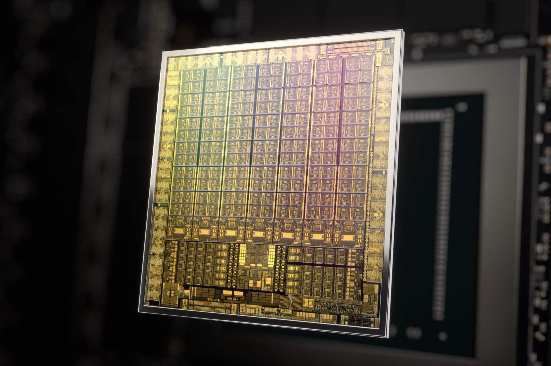
The AD102 chip has 600 mm² after optimisation
According to the leaker Kopite7kimi, Nvidia has also conducted some optimizations in the chip that should save some die area as well as contact pads on the package. The GPUs (including the highest AD102) are said to have completely dropped NVLink connectivity and Nvidia has allegedly also decreased the number of video outputs, however we do not know to how many.
Jensen cost down some small features like NVLINK or extra dp links to reduce pin usage to add gpu power.
— kopite7kimi (@kopite7kimi) March 2, 2022
The need to conserve contacts on the chip package has a reason you might not like much – this is reportedly done in order to free more contact pads for power supply. In other words, for the GPU to be able to consume more power. Overall the AD102 GPU, the highest performance version of the Ada/Lovelace and GeForce RTX 4000, should have a die area of “only” about 600 mm². This is stated directly by the Kopite7kimi, who is very reliable.
More: Insane GPU power consumption? GeForce RTX 4000 might reach a TDP above 800 W
Sources: VideoCardz. XinoAssassin, Kopite7kimi
English translation and edit by Karol Démuth, original text by Jan Olšan, editor for Cnews.cz
⠀