


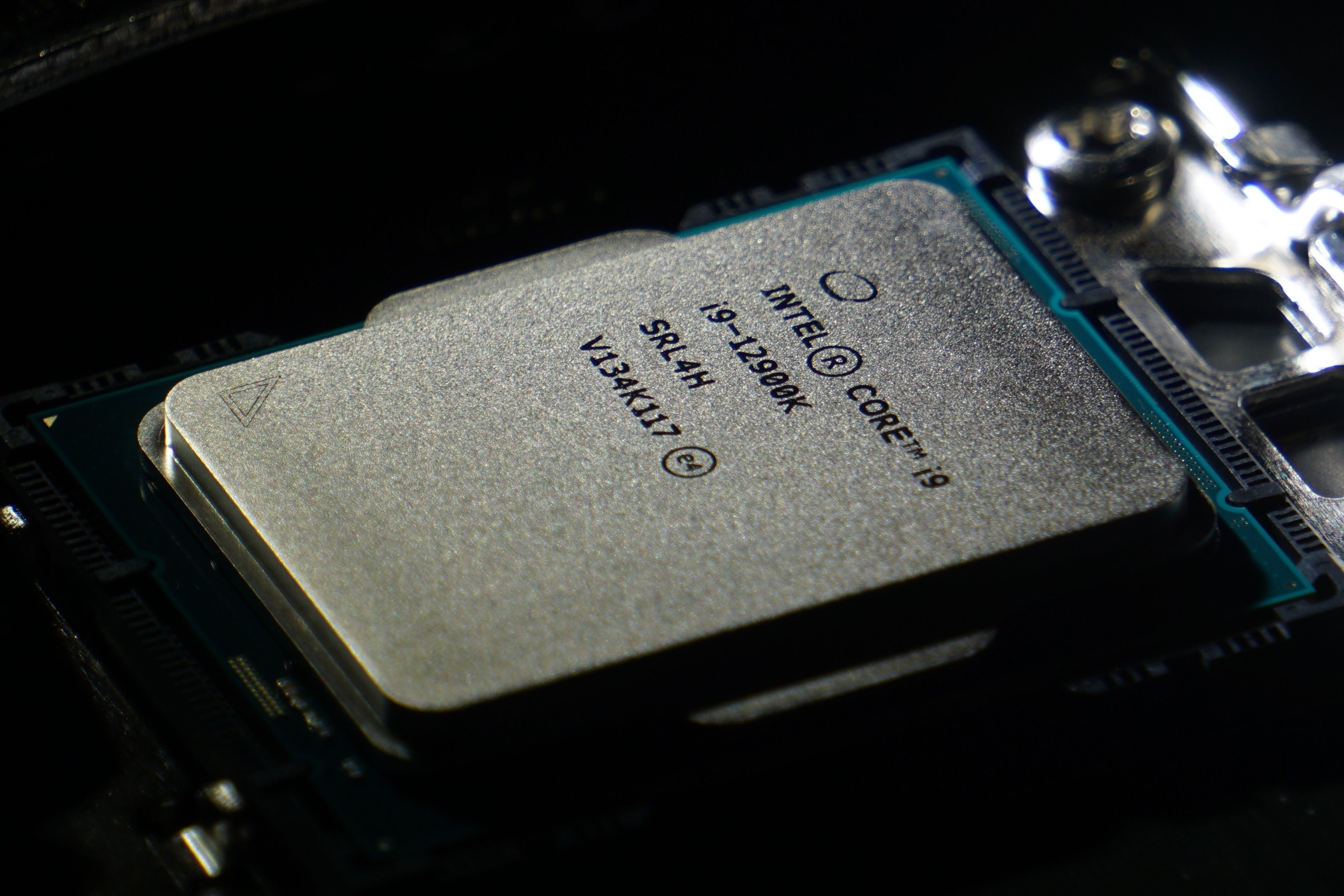
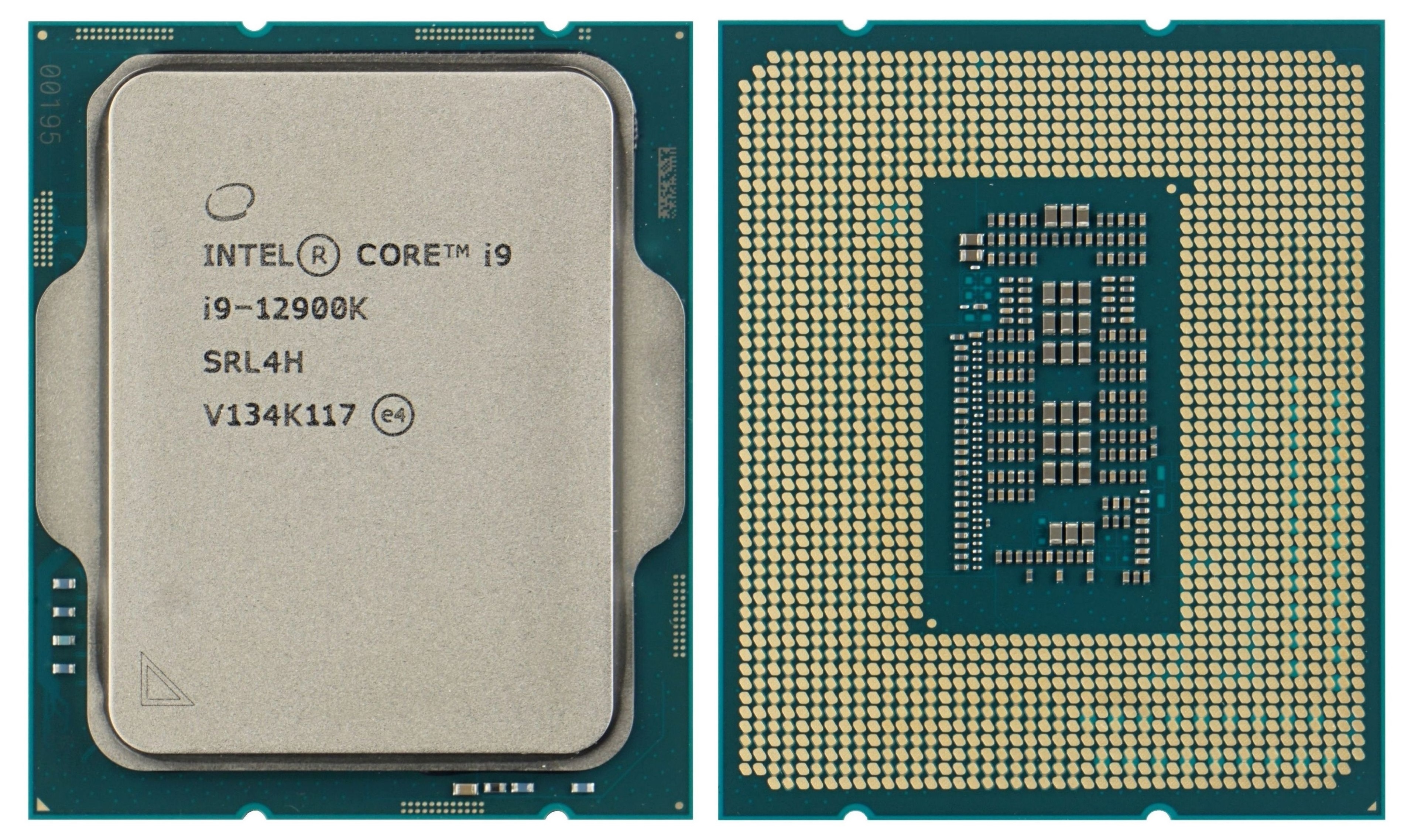
Intel Core i9-12900K in detail
The 12th generation Intel Core processors – Alder Lake is now out and we already have the full-fledged tests for you. These processors are significantly different from the previous ones in many aspects and many things are used “for the first time”. Among them are DDR5 memory support, PCI Express 5.0, 7 nm manufacturing process or hybrid concept of small and large cores. It’s time for a detailed analysis!
Intel Core i9-12900K in detail
We’ve kept you up to date on all the Intel Alder Lake processor news as it’s come out throughout the year. But if you happened to miss something, it doesn’t matter. That’s what this first chapter is for, to give everyone a quick overview of what we’ll be covering next.
Alder Lake-S is the first desktop processor to abandon the 14 nm manufacturing process and switch to modern 7 nm technology (before the renaming it was referred to as 10 nm Enhanced SuperFin). This technology is expected to be very much similar to the TSMC’s 7 nm process used to make AMD processors. So after six years (since Intel Skylake processors) there is finally a big change in the manufacturing process.
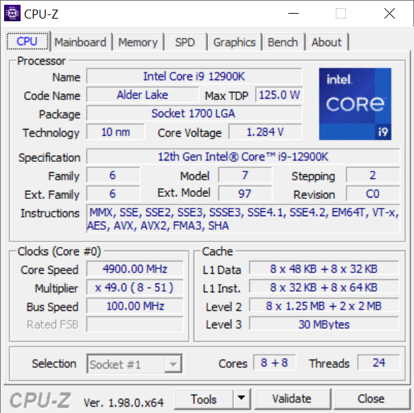
The design of the processors as such is also significantly changed. These are the first processors ever to use a hybrid concept of small and large cores. So something similar to big.LITTLE from ARM. The most powerful of the Alder Lake processors (i.e. the one we’ll be looking at in these tests), the Core i9-12900K, has eight cores, denoted by the letters “P” (Performance) and “E” (Efficient). The Performance cores have high clock speeds and high performance (19% higher than the Rocket Lake and Tiger Lake processors) and support HyperThreading – two threads per core.
The details of the Golden Cove architecture are discussed in detail in this article. The role of these P cores is to provide performance in games and single-threaded applications. The complementary E cores are then also meant to provide high multi-threaded performance, and are secondarily involved in running low-power processes such as services and background tasks. These cores still have relatively good performance (according to Intel, the IPC is similar to Skylake processors), while needing a significantly smaller die area. In terms of space on a silicon chip, four E cores can fit on a single P core, which is why they’re also referred to as “small” cores, for which we also have an architectural analysis.
The smaller manufacturing process also means a smaller surface area of the entire chip ~209 mm² (this is a reduction of more than 24% compared to Rocket Lake), which is naturally associated with poorer heat dissipation from the surface. The chip is soldered to the heat spreader, but this might not be enough for sufficient cooling. Therefore, to maximize heat transfer to the heat sink, Intel has thinned the chip, narrowed the TIM, and in turn increased the thickness of the heat spreader. The latter was also lengthened a bit, which is not primarily due to better cooling properties, but it doesn’t hurt either. The contact area of the IHS is 38 mm in height, but that should be completely covered by the vast majority of heatsink cold plates.
Also new for these processors is the socket (LGA 1700), where the physical dimensions change after 12 years (from LGA 1156 designed for Lynfield processors). So unfortunately you can’t put Alder Lake processors in LGA 1200 and a new motherboard is needed. It can support either the older DDR4 memory (this usually applies to cheaper boards) or the latest DDR5 memory standard. We have tested with these as well and will continue to test in the future. It’s definitely not as much of a scarecrow as is being spouted around the discussion forums. The timings appear to be high, but the important thing is always the end performance, which across all those applications is very respectable.
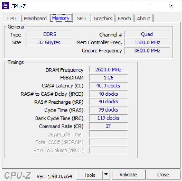
With DDR5 memory, you may be surprised that diagnostic tools report a four-channel connection even if you physically have only two modules. This is due to the fact that while with DDR4 memory, a single DIMM has a 64-bit data width and behaves as a single channel, this has changed with DDR5 memory. Each module is internally divided into two channels of 32 bits each. So if you “dual-channel” two DDR5 modules, from the memory controller’s point of view, it’s a four-channel 32-bit connection (instead of two 64-bit channels). But you don’t have to worry about it, functionally it’s more or less the same as the DDR4 channel.
PCI Express 5.0 support is also being introduced with Alder Lake processors. This new bus will be able to be used on ×16 (or ×8) slots for graphics cards.
- More: Intel Alder Lake CPUs revealed: models, power draws, chipset Z690
- More: Alder Lake and DDR5: XMP 3.0, Dynamic Memory Boost and more
- More: Alder Lake cooling and overclocking news. Solder, auto OC 5,3 GHz
| Manufacturer | Intel | Intel | AMD | |
| Line | Core i9 | Core i9 | Ryzen 9 | |
| SKU | 12900K | 11900K | 5950X | |
| Codename | Alder Lake | Rocket Lake | Vermeer | |
| CPU microarchitecture | Golden Cove (P) + Gracemont (E) | Cypress Cove | Zen 3 | |
| Manufacturing node | 7 nm | 14 nm | 7 nm + 12 nm | |
| Socket | LGA 1700 | LGA 1200 | AM4 | |
| Launch date | 11/04/ 2021 | 03/30/2021 | 11/06/2020 | |
| Launch price | 589 USD | 539 USD | 799 USD | |
| Core count | 8+8 | 8 | 16 | |
| Thread count | 24 | 16 | 32 | |
| Base frequency | 3.2 GHz (P)/2.4 GHz (E) | 3.5 GHz | 3.7 GHz | |
| Max. Boost (1 core) | 5.2 GHz (P)/3.9 GHz (E) | 5.3 GHz | 4.90 GHz (5.05 GHz unofficially) | |
| Max. boost (all-core) | 4.9 GHz (P)/3.7 GHz (E) | 4.8 GHz | N/A | |
| Typ boostu | TBM 3.0 | TBM 3.0, TVB, ABT | PB 2.0 | |
| L1i cache | 32 kB/P core, 64 kB/E core | 32 kB/core | 32 kB/core | |
| L1d cache | 48 kB/P core, 32 kB/E core | 48 kB/core | 32 kB/core | |
| L2 cache | 1.25 MB/P core, 2× 2 MB/4 E cores | 512 kB/core | 512 kB/core | |
| L3 cache | 1× 30 MB | 1× 16 MB | 2× 32 MB | |
| TDP | 125 W | 125 W | 105 W | |
| Max. power draw during boost | 241 W (PPT) | 251 W (PL2) | 142 W (PPT) | |
| Overclocking support | Yes | Yes | Yes | |
| Memory (RAM) support | DDR5-4800/DDR4-3200 | DDR4-3200 | DDR4-3200 | |
| Memory channel count | 2× 64 bit | 2× 64 bit | 2× 64 bit | |
| RAM bandwidth | 76.8 GB/s/51.2 GB/s | 51.2 GB/s | 51.2 GB/s | |
| ECC RAM support | No | No | Yes but unofficial | |
| PCI Express support | 5.0/4.0 | 4.0 | 4.0 | |
| PCI Express lanes | ×16 (5.0) + ×4 (4.0) | ×16 + ×4 | ×16 + ×4 | |
| Chipset downlink | DMI 4.0 ×4 | DMI 3.0 ×8 | PCIe 4.0 ×4 | |
| Chipset downlink bandwidth | 16.0 GB/s duplex | 8.0 GB/s duplex | 8,0 GB/s duplex | |
| BCLK | 100 MHz | 100 MHz | 100 MHz | |
| Die size | ~209 mm² | 276.4 mm² | 2× 80.7 mm² + 125 mm² | |
| Transistor count | ? mld. | ? bn. | 2× 4.15 + 2.09 bn. | |
| TIM used under IHS | Solder | Solder | Solder | |
| Boxed cooler in package | No | No | No | |
| Instruction set extensions | SSE4.2, AVX2, FMA, SHA, VNNI (256-bit), GNA 2.0, VAES (256-bit) | SSE4.2, AVX2, FMA, AVX-512, SHA, VNNI, GNA 2.0 | SSE4.2, AVX2, FMA, SHA | |
| Virtualization | VT-x, VT-d, EPT | VT-x, VT-d, EPT | AMD-V, IOMMU, NPT | |
| Integrated GPU | UHD 770 | UHD 750 | N/A | |
| GPU architecture | Xe LP (Gen. 12) | Xe LP (Gen. 12) | – | |
| GPU: shader count | 256 | 256 | – | |
| GPU: TMU count | 16 | 16 | – | |
| GPU: ROP count | 8 | 8 | – | |
| GPU frequency | 350–1550 MHz | 350–1300 MHz | – | |
| Display outputs | DP 1.4a, HDMI 2.0b | DP 1.4a, HDMI 2.0b | – | |
| Max. resolution | 5120 × 3200 px (60 Hz) | 5120 × 3200 px (60 Hz) | – | |
| HW video encode | HEVC, VP9 | HEVC, VP9 | – | |
| HW video decode | AV1, HEVC, VP9 | AV1, HEVC, VP9 | – |
- Contents
- Intel Core i9-12900K in detail
- Methodology: performance tests
- Methodology: how we measure power draw
- Methodology: temperature and clock speed tests
- Test setup
- 3DMark
- Assassin’s Creed: Valhalla
- Borderlands 3
- Counter-Strike: GO
- Cyberpunk 2077
- DOOM Eternal
- F1 2020
- Metro Exodus
- Microsoft Flight Simulator
- Shadow of the Tomb Raider
- Total War Saga: Troy
- Overall gaming performance
- Gaming performance per euro
- PCMark
- Web performance
- 3D rendering: Cinebench, Blender, ...
- Video 1/2: Adobe Premiere Pro
- Video 1/2: DaVinci Resolve Studio
- Graphic effects: Adobe After Effects
- Video encoding
- Audio encoding
- Broadcasting (OBS a Xsplit)
- Photos 1/2: Adobe Photoshop a Lightroom
- Photos 2/2: Affinity Photo, Topaz Labs AI apps, ZPS X, ...
- (De)compression
- (De)cryption
- Numerical computing
- Simulations
- Memory and cache tests
- Processor power draw curve
- Average processor power draw
- Performance per watt
- Achieved CPU clock speed
- CPU temperature
- Conclusion

There is a small error, the i9-12900k is manufactured in 10 nm (intel 7).
We decided to treat is as a 7nm process, since it more or less reflects reality, and Intel more or less wants it to be treated like that. The “Intel 7” does not actually say “nm” anywhere, but the follow up processes will actually be marketed like that. The 20A and 18A processes actually refer to Angstroms, which are non-SI units meaning 0.1nm. So those processes are officially 2nm and 1.8nm when it comes to Intel messaging.
But when we put that aside, in my opinion it is more useful than not to use “7nm” for the Alder Lake chips. Intel’s 10nm process was in fact roughly comparable to TSMC’s N7 (7nm) process, once Intel got rid of the problems (in the SuperFin or Enhanced SuperFin versions). It is not equal parity in everything, but these technologies can be considered competitive. Calling it 10nm makes it look the process is worse than it is if people assume it is similar to 10nm Samsung or TSMC process node.
We would basically have to keep reminding people that “Intel’s 10nm is on the level of TSMC’s 7nm”. And it’s not practical to to keep repeating that every time. Ideally this should have been done earlier so that the products were not referred to as 10nm for 2-3 years in press.
In isolation, the process renaming would not be a good thing, but in a way, Intel only did what TSMC and Samsung did before them. Their processes could be said to be renamed already, so Intel just caught up with that marketing. (Not saying they are at the exact same tech level, but it’s in the ballpark for better or worse).