To provide the best experiences, we and our partners use technologies like cookies to store and/or access device information. Consenting to these technologies will allow us and our partners to process personal data such as browsing behavior or unique IDs on this site and show (non-) personalized ads. Not consenting or withdrawing consent, may adversely affect certain features and functions.
Click below to consent to the above or make granular choices. Your choices will be applied to this site only. You can change your settings at any time, including withdrawing your consent, by using the toggles on the Cookie Policy, or by clicking on the manage consent button at the bottom of the screen.
Technické uloženie alebo prístup sú nevyhnutne potrebné na legitímny účel umožnenia použitia konkrétnej služby, ktorú si účastník alebo používateľ výslovne vyžiadal, alebo na jediný účel vykonania prenosu komunikácie cez elektronickú komunikačnú sieť.
Technické uloženie alebo prístup je potrebný na legitímny účel ukladania preferencií, ktoré si účastník alebo používateľ nepožaduje.
Technické úložisko alebo prístup, ktorý sa používa výlučne na štatistické účely.
Technické úložisko alebo prístup, ktorý sa používa výlučne na anonymné štatistické účely. Bez predvolania, dobrovoľného plnenia zo strany vášho poskytovateľa internetových služieb alebo dodatočných záznamov od tretej strany, informácie uložené alebo získané len na tento účel sa zvyčajne nedajú použiť na vašu identifikáciu.
Technické úložisko alebo prístup sú potrebné na vytvorenie používateľských profilov na odosielanie reklamy alebo sledovanie používateľa na webovej stránke alebo na viacerých webových stránkach na podobné marketingové účely.


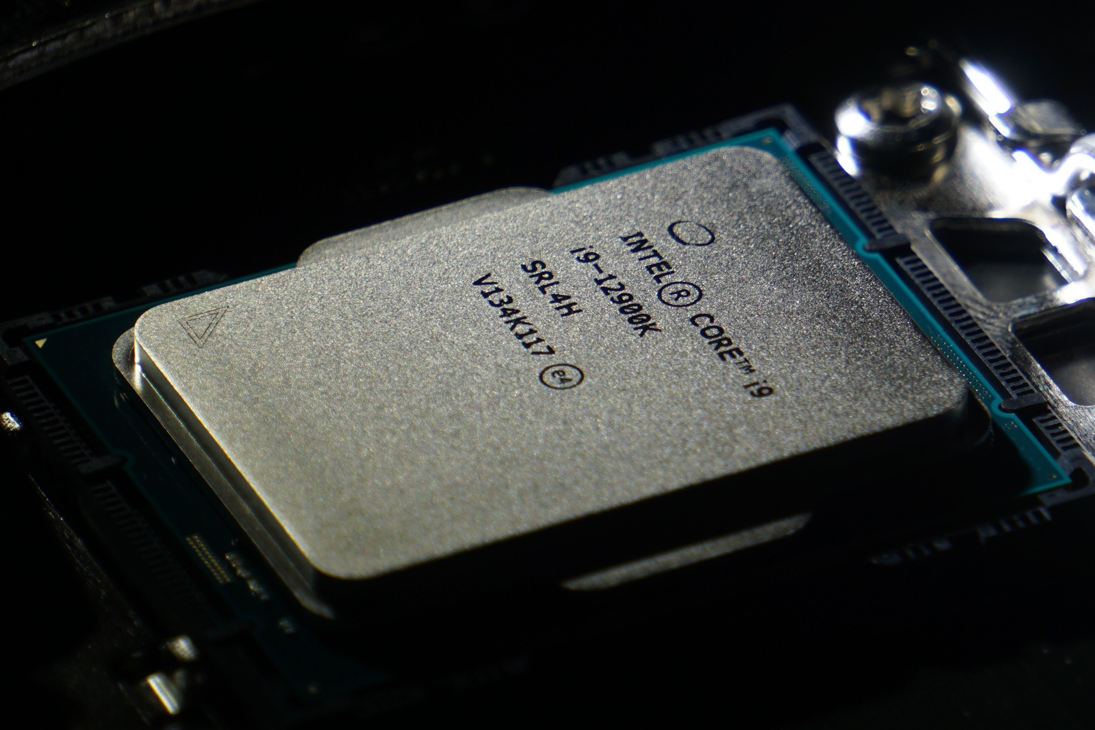

There is a small error, the i9-12900k is manufactured in 10 nm (intel 7).
We decided to treat is as a 7nm process, since it more or less reflects reality, and Intel more or less wants it to be treated like that. The “Intel 7” does not actually say “nm” anywhere, but the follow up processes will actually be marketed like that. The 20A and 18A processes actually refer to Angstroms, which are non-SI units meaning 0.1nm. So those processes are officially 2nm and 1.8nm when it comes to Intel messaging.
But when we put that aside, in my opinion it is more useful than not to use “7nm” for the Alder Lake chips. Intel’s 10nm process was in fact roughly comparable to TSMC’s N7 (7nm) process, once Intel got rid of the problems (in the SuperFin or Enhanced SuperFin versions). It is not equal parity in everything, but these technologies can be considered competitive. Calling it 10nm makes it look the process is worse than it is if people assume it is similar to 10nm Samsung or TSMC process node.
We would basically have to keep reminding people that “Intel’s 10nm is on the level of TSMC’s 7nm”. And it’s not practical to to keep repeating that every time. Ideally this should have been done earlier so that the products were not referred to as 10nm for 2-3 years in press.
In isolation, the process renaming would not be a good thing, but in a way, Intel only did what TSMC and Samsung did before them. Their processes could be said to be renamed already, so Intel just caught up with that marketing. (Not saying they are at the exact same tech level, but it’s in the ballpark for better or worse).