


Photos 2/2: Affinity Photo, Topaz Labs AI apps, ZPS X, ...
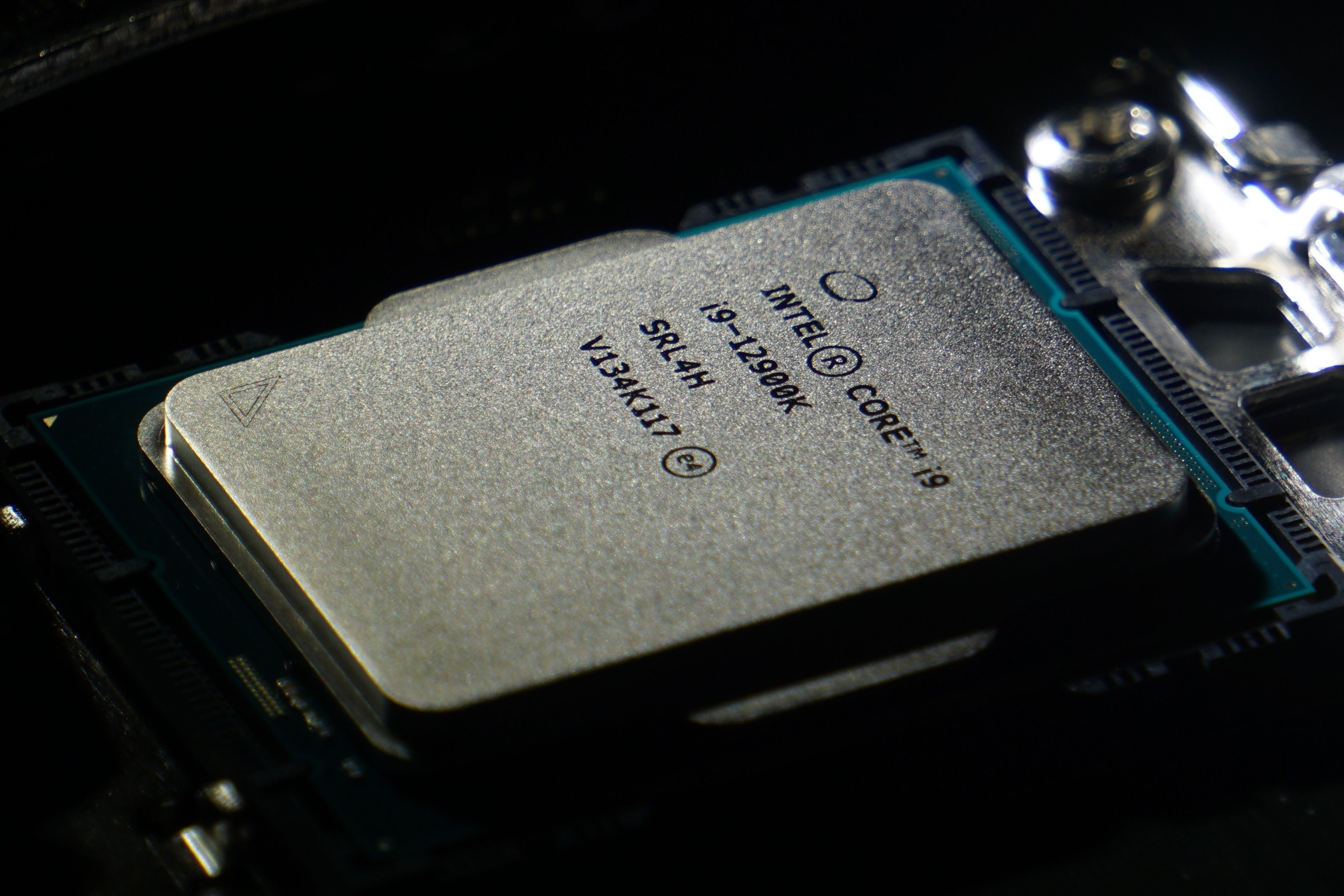
The 12th generation Intel Core processors – Alder Lake is now out and we already have the full-fledged tests for you. These processors are significantly different from the previous ones in many aspects and many things are used “for the first time”. Among them are DDR5 memory support, PCI Express 5.0, 7 nm manufacturing process or hybrid concept of small and large cores. It’s time for a detailed analysis!
Affinity Photo (benchmark)
Test environment: built-in benchmark.
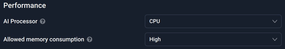
Topaz Labs AI apps
Topaz DeNoise AI, Gigapixel AI and Sharpen AI. These single-purpose applications are used for restoration of low-quality photos. Whether it is high noise (caused by higher ISO), raster level (typically after cropping) or when something needs extra focus. The AI performance is always used.
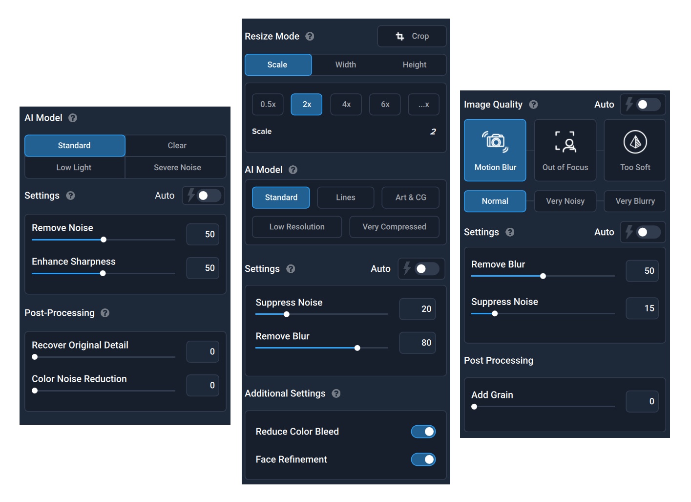
Test environment: As part of batch editing, 42 photos with a lower resolution of 1920 × 1280 px are processed, with the settings from the images above. DeNoise AI is in version 3.1.2, Gigapixel in 5.5.2 and Sharpen AI in 3.1.2.
XnViewMP

Test environment: XnViewMP is finally a photo-editor for which you don’t have to pay. At the same time, it uses hardware very efficiently. In order to achieve more reasonable comparison times, we had to create an archive of up to 1024 photos, where we reduce the original resolution of 5472 × 3648 px to 1980 × 1280 px and filters with automatic contrast enhancement and noise reduction are also being applied during this process. We use 64-bit portable version 0.98.4.
Zoner Photo Studio X
Test environment:In Zoner Photo Studio X, we convert 42 .CR2 (RAW Canon) photos to JPEG while keeping the original resolution (5472 × 3648 px) at the lowest possible compression, with the ZPS X profile ”high quality for archival”.
- Contents
- Intel Core i9-12900K in detail
- Methodology: performance tests
- Methodology: how we measure power draw
- Methodology: temperature and clock speed tests
- Test setup
- 3DMark
- Assassin’s Creed: Valhalla
- Borderlands 3
- Counter-Strike: GO
- Cyberpunk 2077
- DOOM Eternal
- F1 2020
- Metro Exodus
- Microsoft Flight Simulator
- Shadow of the Tomb Raider
- Total War Saga: Troy
- Overall gaming performance
- Gaming performance per euro
- PCMark
- Web performance
- 3D rendering: Cinebench, Blender, ...
- Video 1/2: Adobe Premiere Pro
- Video 1/2: DaVinci Resolve Studio
- Graphic effects: Adobe After Effects
- Video encoding
- Audio encoding
- Broadcasting (OBS a Xsplit)
- Photos 1/2: Adobe Photoshop a Lightroom
- Photos 2/2: Affinity Photo, Topaz Labs AI apps, ZPS X, ...
- (De)compression
- (De)cryption
- Numerical computing
- Simulations
- Memory and cache tests
- Processor power draw curve
- Average processor power draw
- Performance per watt
- Achieved CPU clock speed
- CPU temperature
- Conclusion


There is a small error, the i9-12900k is manufactured in 10 nm (intel 7).
We decided to treat is as a 7nm process, since it more or less reflects reality, and Intel more or less wants it to be treated like that. The “Intel 7” does not actually say “nm” anywhere, but the follow up processes will actually be marketed like that. The 20A and 18A processes actually refer to Angstroms, which are non-SI units meaning 0.1nm. So those processes are officially 2nm and 1.8nm when it comes to Intel messaging.
But when we put that aside, in my opinion it is more useful than not to use “7nm” for the Alder Lake chips. Intel’s 10nm process was in fact roughly comparable to TSMC’s N7 (7nm) process, once Intel got rid of the problems (in the SuperFin or Enhanced SuperFin versions). It is not equal parity in everything, but these technologies can be considered competitive. Calling it 10nm makes it look the process is worse than it is if people assume it is similar to 10nm Samsung or TSMC process node.
We would basically have to keep reminding people that “Intel’s 10nm is on the level of TSMC’s 7nm”. And it’s not practical to to keep repeating that every time. Ideally this should have been done earlier so that the products were not referred to as 10nm for 2-3 years in press.
In isolation, the process renaming would not be a good thing, but in a way, Intel only did what TSMC and Samsung did before them. Their processes could be said to be renamed already, so Intel just caught up with that marketing. (Not saying they are at the exact same tech level, but it’s in the ballpark for better or worse).