
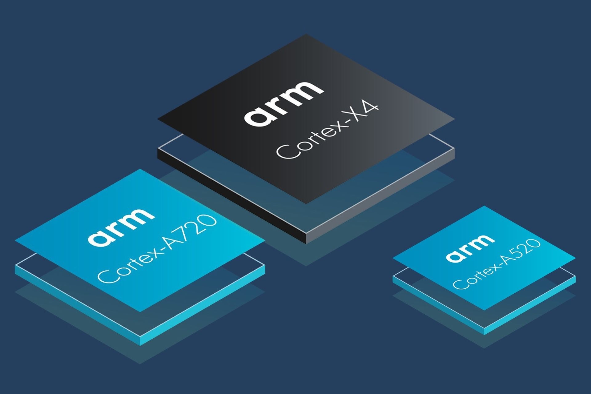
ARM has been releasing a new generation of processor cores every year lately. This year will be no different (except for the Computex timing). ARM has unveiled a complete line of new architectures: a new Cortex-X4 “prime” big core for maximum single-threaded performance, a new medium Cortex-A720 core whose role is to provide multi-threaded performance (like Intel’s E-Core), and finally a new low-power Cortex-A520 little core.
The most powerful core in the generation will be the Cortex-X4, the successor to the previous Cortex-X3. This core will aim to provide single-threaded performance in mobile devices and thus there will often only be one in the whole SoC (this may however be different in laptop chips). This is because this core is not tuned to maximize performance/area ratio and performance/power draw ratio.
The cores in the X line of Cortex are designed to have the highest single-threaded performance possible, even at the cost of degraded power efficiency and area efficiency. While this approach helps single-threaded applications, multi-threaded applications would fare worse if constrained to a certain power limit with only Cortex-X cores compared to using several (potentially higher count) of medium Cortex-A cores with the same power draw. Thus, the big and medium cores are specialized for different scenarios and are complementary in a hybrid architecture. Or at least that is the theory.

The Cortex-X4 is the most powerful ARM Holdings’ core to date. This is of course the case with these cores every year as performance keeps increasing between generations. But in this case, it’s not just about real world app performance. The core is actually radically more powerful (wider) in terms of architectural design, going significantly further than anything before it.
More ALUs than Apple
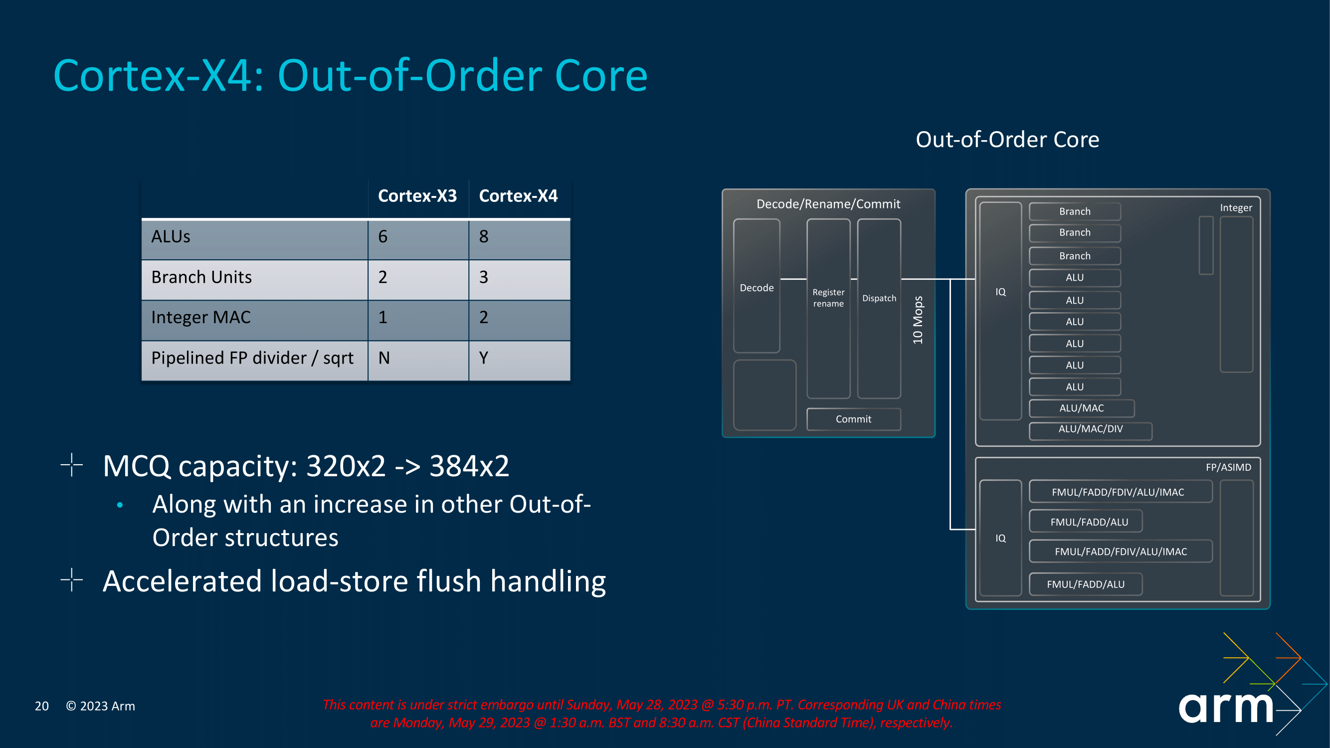
This core has eight integer ALUs (versus six in Cortex-X3 or in Apple’s cores and mere four in AMD Zen 4). Six ALUs are capable of common simple instructions with one cycle latency, the other two are able to execute more complex multi-cycle instructions and have integer MAC functionality (whereas only one of these two complex ALUs offered it in Cortex-X3). The integer divider is still only implemented in one of the complex ALUs. At the same time, the number of branch units that are separate has been increased from two to three (which is also more than in Apple cores and Zen 4, which have only two).


On the other hand, apparently no units have been added in the FPU part of the core, it still has only four pipelines, and apparently the SIMD pipelines continue to only be 128-bit wide (compared to 256 to 512-bit unit widths on x86 processors). So the performance of the Neon and SVE/SVE2 instructions probably won’t increase much (unless improvements in other parts of the core help their loops). The only major change from Cortex-X3 seems to be that the floating-point divider will be pipelined (which it wasn’t before). This will increase the performance of these instructions by quite a bit. However, their use is not that common, because programmers usually try to avoid them when optimizing due to the high cost.
The core now has eight decoders, completely dropping the uOP cache
But ARM is also betting on core widening in other pipeline stages, especially in the frontend. The processor has eight parallel instruction decoders, which is also a record number for ARM’s cores (Apple also has eight decoders). These decoders can deliver eight instructions per cycle to the following processing stages. Dispatch then supports up to 10 micro-ops per cycle (not all instructions are decoded to one micro-op).
ARM also seems to have shortened the processor pipeline, which goes a bit against the evolutionary trend of other architectures where additional stages tend to be added (which more accurately means that the processing steps that perform their work in one cycle in a a shorter-pipeline CPU are split into multiple cycles). The Cortex-X3 had an 11-stage pipeline (which was the amount of cycles that a mispredicted branch would cost – although the cost was only 9 cycles when getting micro-ops from the uOP cache). In contrast, the Cortex-X4 only ever has a penalty of 10 cycles and a 10-stage pipeline.
More stages will usually allow CPU cores to achieve higher clock speeds, but the penalty for brach mispredicts increases. And when the clock speed gets higher, so does the power draw. ARM’s pipeline shortening probably contributes to higher core IPC at low power, but it will be at the cost of a low clock speed ceiling.
The aforementioned micro-op (uOP) cache, which caches micro-ops (already decoded instructions), has been removed in the Cortex-X4, which is quite a major change. However, this was already hinted at in Cortex-X3, which reduced its capacity. So what’s this all about? For example, in x86 processors, decoders are very complex and have higher power draw due to the complexity of the instruction set, and the variable instruction length also makes it harder to have multiple instructions in parallel. Intel and AMD have responded to this by introducing a new cache (uOP, micro-op cache) that caches already decoded instructions. This takes advantage of the fact that the processor is processing constantly repeating loops, where it is possible to skip decoding and reuse a decoded instruction from a previous pass. It has been reported that the hit rate of these caches can be as high as 80%, so the problems and limits of x86 decoders do not really exist for 80% of the execution time.
Apple never had a micro-op cache, but ARM used it for Cortex-A77 to X3 cores because apparently it still reduced power draw despite the ARM instruction set being easier to decode. But this reportedly changed with the removal of 32-bit instruction set support when the core became purely ARMv8/ARMv9. This greatly reduced the decoder area and the Cortex-X3 core therefore opted for more decoders and the micro-op cache got smaller. Now ARM went further down the path and completely replaced this cache with even more decoders.
As already mentioned, there are eight decoders and they can process eight instructions per cycle and deliver up to 10 operations to the next processing stages (so-called dispatch). In comparison Cortex-X3 had a maximum output of six operations per cycle from the decoders or eight operations from the uOP cache. The previous fetch phase, which takes instructions from the L1 instruction cache and sends them to the decoders in the queue, has also been newly enhanced to deliver up to 10 instructions per cycle.
The complexity of the out-of-order architecture is not only measured by the “width” (number of units in parallel), but also by the depth of the buffers and queues the processor uses. In these queues, the processor can shift and reshuffle operations around to improve performance by optimally utilizing as many units as possible at once. This works better the larger the “window” of code the processor can handle. This window is usually named ReOrder Buffer (ROB), but ARM calls it Micro-op Commit Queue (MCQ) for this core. The Cortex-X4 increased the depth of this queue by 20% – from 320 to 384 instructions (or at this stage, micro-ops). If two micro-ops are fused in the previous processing stage, they occupy only one entry, which is why ARM states that the MCQ capacity is 384×2. This does not mean that the “window” has 768 entries. For comparison – in AMD Zen 4 the ROB has only 320 entries (AMD is quite minimalistic in this area, Zen 3 had only 256-entry ROB). On the contrary Intel Golden Cove / Raptor Cove has 512 entries and for Apple cores apparently the depth should be over 600 (these are unofficial estimates, because the company itself does not disclose anything).

Larger L2 cache without higher latency
The processor also has improved branch predictors, with particular effort being spent on conditional branches. Similarly, the prefetchers have been improved. Both of these are areas where incremental improvements tend to be made in all new architectures, and this core is no exception. The Cortex-X4 has been given a new temporal L1 cache prefetcher, and the L1 cache should have a reduced incidence of inter-bank conflicts. The L1 TLB for data has also been increased from 48 to 96 entries.
Another improvement is the support for 2MB L2 cache, which has been brought closer to the execution units in the physical layout and probably thanks to that it has maintained the same latency despite the higher capacity. This should hopefully result in a pure performance improvement per 1 MHz without regressions in some algorithms that are latency dependent but do not benefit from the higher capacity. For the L2 cache, the data filling and replacement policy has also been modified.
Although the Cortex-X3 cores are not optimized for the smallest possible area, as already mentioned, this criterion is still quite accentuated in all ARM designs (compared to Apple cores, for example). This is probably due to the preferences of mobile SoC manufacturers, who are under price pressure and the production cost of the chip is important to them, unlike to Apple. So the Cortex-X4 is still relatively small, according to ARM it will only need about 10% more area than the previous Cortex-X3 (when using the same manufacturing process and the same L2 cache capacity).
IPC and performance
The result of all this is a core that is supposed to have up to 15% better “IPC” or performance per 1 MHz than the Cortex-X3. This is for the same CPU clock speed, the same L3 cache, and the same memory bandwidth and latency. It should be said that these are not results measured on real hardware, but merely an estimate based on simulation.
Realistically, of course, the increase will be different from application to application. The IPC increases seem to be higher in multi-threaded applications (Speedometer2: +24%), but in single-threaded applications, on the other hand, the improvement may be lower. Geekbench 5 and Geekbench 6 seem to have IPC increases of only about +7% to +8%. What comes closest to the claimed average improvement off all the tasks that ARM shows in the slides is SPEC2017 (SPECRate2017_int_base), which shows an IPC improvement of +14%. The SPEC benchmarks have always shown good (and perhaps above average vs. other tasks) increases with ARM processors, whatever the reason.

Alternatively, the core should achieve the same performance as Cortex-X3 with up to 40% lower power draw (thanks to the higher IPC it can run at a lower clock speed). In practice, however, manufacturers will choose to increase performance instead of reducing power draw, so you won’t see much of a reduction in power draw in practice.
According to ARM, the Cortex-X4 should reach a clock speed of up to 3.4 GHz. So it won’t scale very high in this regard – as the small number of pipeline stages suggests – which in turn will limit absolute performance somewhat. After all, high IPC is only one part of the equation. For example, Apple’s cores are already reaching higher clock speeds, not to mention Intel and AMD processors, which are already in the 5.5-6.0 GHz band, which automatically gives 60–75% extra performance just from the clock difference.
DSU-120
To interconnect these (and their little sibling) cores in chips, the DSU-120 logic¨is provided. It will support up to 14 cores in total and up to 32MB of shared L3 cache. So apparently configurations like 4 big cores + 8 medium cores + 2 little cores could be available. A combination of 10 Cortex-X4 cores and four Cortex-A720 cores is also explicitly supported, according to ARM. Something like it could be used by high-performance laptop processors.

The article continues on the next page.