


AMD has unveiled its future processor roadmaps during Financial Analyst Day last week, officially revealing the Zen 7 CPU architecture plans for the first time. The company hasn’t said much more yet, but Moore’s Law is Dead published a video providing further details about Zen 7 and a preview of what processors with these cores might look like, around the same time. While it’s unverified information, it’s quite interesting.
At least a portion of the Zen 7 generation processors will again be chiplet-based. According to Moore’s Law is Dead, AMD is will keep using CPU chiplets that will be shared across multiple products—desktop, server, and some notebook processors. The main CPU chiplet (CCD) with the codename “Silverton” will provide 16 Zen 7 cores, as has previously shown up in leaks. Zen 7 will thus again increase the core count somewhat right after from Zen 6 generation, which itself increases the core count per CPU chiplet from 8 to 12).
The Zen 7 core reportedly has the internal codename Prometheus, according to Moore’s Law is Dead. The primary manufacturing process for it, meaning the one used for the mentioned 16-core chiplet, is a 1.4nm technology, specifically TSMC’s A14 process. This means it won’t be the 1.6nm A16 process, which is actually a variant of the 2nm process enhanced with backside power delivery technology. In contrast, the 1.4nm A14 process is a completely new generation, but without backside power delivery. AMD apparently doesn’t want to deploy this technology for its mainstream-market processors yet.
Based on document fragments shown by MLID, the CPU chiplet with 16 cores could have 19 metal layers, use HP libraries, and the estimated die area is 98 mm². This is significantly larger than today’s CPU chiplets used in Ryzen processors, suggesting that processors with Zen 7 cores coul be easier to cool—that is, when talking about higher core count configurations.
Smaller eight-core chiplet
AMD is also reportedly preparing an eight-core chiplet codenamed “Silverking” for cheaper processors, which will again be very small and thus potentially suffer from high temperatures. This chiplet will also be used in laptop processors.
The sixteen-core chiplet will support the mounting of a 3D V-Cache die underneath the core die, for use in gaming X3D processors. The capacity of the add-on chiplet will be 160 MB and it will be manufactured on a 4nm process (TSMC N4P). The total L3 cache for a gaming 16-core part would therefore be 224 MB. Only a single layer of cache is planned, not multiple layers. For the 8-core CPU chiplet, 3D V-Cache option is apparently not planned.
Larger cache and matrix instructions?
Zen 7 should, according to Moore’s Law is Dead, have larger private caches per core—2MB L2 cache for each core instead of the 1 MB in today’s cores. The L3 cache will remain fundamentally the same in its basic configuration, supposedly corresponding to 4 MB per core. However, because the core count is increasing, the 16-core chiplet will have 64 MB of L3 cache (but the 8-core chiplet will likely retain today’s 32 MB per-CCD capacity).
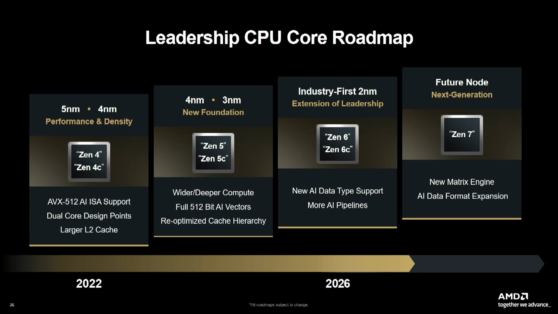
The Zen 7 core in the high-performance desktop version will again feature 512-bit SIMD units for AVX-512 instructions. But the documents also allegedly promise AMX instructions support, providing AI acceleration capability within the cores. Specifically, they mention the designation ACE. When Intel and AMD recently announced plans to standardize matrix instructions in all x86 processors, it was ACE that was used as the announced designation for them.
We assume ACE will be based on the AMX instruction set already present in the last few Intel Xeon server processors. The documents aparently state “½ ACE”, which might perhaps mean the implementation has reduced performance, similar to how there are AVX-512 implementations with half-width units and thus half the raw throughput.
IPC increase?
Moore’s Law is Dead also provides alleged “projections” for Zen 7 performance. Here it must be noted that any data of this type is quite likely to be mere speculations (in other words, made up) this far out. The same YouTuber has in the past cited figures for alleged single-thread performance or IPC increases that, upon release, turned out to be extremely off the mark, for example for Arrow Lake processors. Therefore, we present the following information just as a curiosity; consider it to be claims by this particular YouTuber, while we cannot be sure if they are truly from any AMD documents or if they are valid. Furthermore, it’s important to remember that the launch of processors with the Zen 7 architecture might still be up to three years away. Any internal performance estimates would thus be merely projections at this point, which the final production silicon may not fulfill.
Moore’s Law is Dead claims that Zen 7 will bring an IPC (performance per 1 MHz clock speed) increase between 15–25 % compared to Zen 6. As you can see, the range is very wide, so this number isn’t overly useful, and the authenticity of the information isn’t very testable, as it’s quite probable that the officially stated figure will end up somewhere in this range anyway. According to other data, Zen 7 is also said to have 15–25 % higher single-core performance in SPECINT 2017 versus Zen 6, and 16–20 % higher per-core performance in “non-gaming applications” (these numbers are not pure IPC; here we are likely talking about results combining IPC increase and potential clock speed increase).
Zen 7 in laptops: Grimlock Point and Grimlock Halo
Following the Medusa Point and Medusa Halo APUs, which will be based on Zen 6, the next APU family based on Zen 7 will reportedly consist of processors named Grimlock Halo and Grimlock Point, according to Moore’s Law is Dead. The Halo version is a high-performance, extreme variant corresponding to today’s Ryzen AI Max series (which in the Zen 5 generation are designated “Strix Halo”), while Grimlock Point would be the standard mainstream mobile Ryzen AI processor.
The mainstream Grimlock Point (or Grimlock 1) version is allegedly composed of an I/O or SoC die containing 12 cores (4x Zen 7 and 8x Zen 7c) plus an unknown number of low-power LP cores (these will probably have a similar function to those in Intel processors), perhaps two or four. Cheaper processors will offer only this, but more powerful models will additionally feature a added 1.4nm Silverking chiplet with another 8 Zen 7 cores. This configuration would thus be up to twenty cores (12x Zen 7, 8x Zen 7c), plus some LP cores. So the total could likely be 24 cores.
Unfortunately, information about the integrated GPU is still missing. AMD is also said to have lower-end, cheaper models with smaller chips in preparation, but their details haven’t leaked yet either.
The extreme high-performance Grimlock Halo version will be based on an I/O or SoC die with 20 cores (8x Zen 7, 12x Zen 7c) and again an unknown number of LP cores. To this base, it will be possible to mount one or two Silverking chiplets, i.e., up to 8–16 additional cores. The maximum core count for a Halo processor would therefore be 36 (24x Zen 7 and 12x Zen 7c), plus LP cores.
Information about the integrated graphics is unfortunately also missing.

Desktop: Grimlock Ridge
The desktop version of the processors will be named Grimlock Ridge. This design is apparently still intended for the AM5 socket, meaning it should be possible to install Zen 7 as upgrade into today’s motherboards if all goes well. Grimlock Ridge will use the same I/O die that will be used in the desktop processors with Zen 6 cores (“Olympic Ridge”). AMD will thus stick to its current strategy where one I/O die gives rise to two processor generations by swapping the CPU chiplets.
Grimlock Ridge will again allow the use of two CPU chiplets in the processor for the AM5 socket. The maximum configuration will therefore likely be 32 cores / 64 threads and 128 MB of cache (or up to 448 MB with 3D V-Cache). However, configurations with 24 cores are also expected in the lineup, and when using only one chiplet, configurations with 16 and 12 cores.
Low-end models will be based on (apparently always just one) Silverking chiplet with eight cores. From this, AMD will presumably also be able to derive processors with eight and six cores (using harvested chips with defects in a core or two).
Server processors with more than 256 cores
The server version of Zen 7 is reportedly codenamed Steamboat. It uses a chiplet with 33 Zen 7 cores (it’s possible that one is intended as a spare, so in actual products, typically only 32 will be active). Processors will be able to use 2, 4, 6, or 8 chiplets, meaning a maximum of up to 264 cores (or 256, if one is always a spare). These processors are also expected to use some form of 3D V-Cache, providing a capacity of up to 7 MB of L3 cache per core (thus up to 1848 MB for 264 cores).
In this case, all L3 cache would apparently be on a separate chiplet, with none present on the CPU chiplet itself (which would be a change from the current 3D V-Cache concept). 7 MB per core is a somewhat peculiar number; MLID states it could be changed to 8 MB. Theoretically, the reason for this odd number could again be because part of the capacity is reserved for yield reasons. Or it’s possible that 8 MB per core didn’t work out dimensions-wise. Since this cache will be layered underneath the CPU cores, the block dimensions must match the cores themselves, and it’s possible that an 8MB block ended up exceeding the planned area of a Zen 7 core.
Roughly in three years?
The launch of processors with the Zen 7 architecture could presumably occur in 2028. We are likely not talking about the very beginning of the year. However, official information regarding the intended launch timeframe is missing. Unfortunately, it’s not clear if we’re looking at the start of the year, the second half (more likely), or perhaps the end of the year.
Source: Moore’s Law is Dead
English translation and edit by Jozef Dudáš
⠀