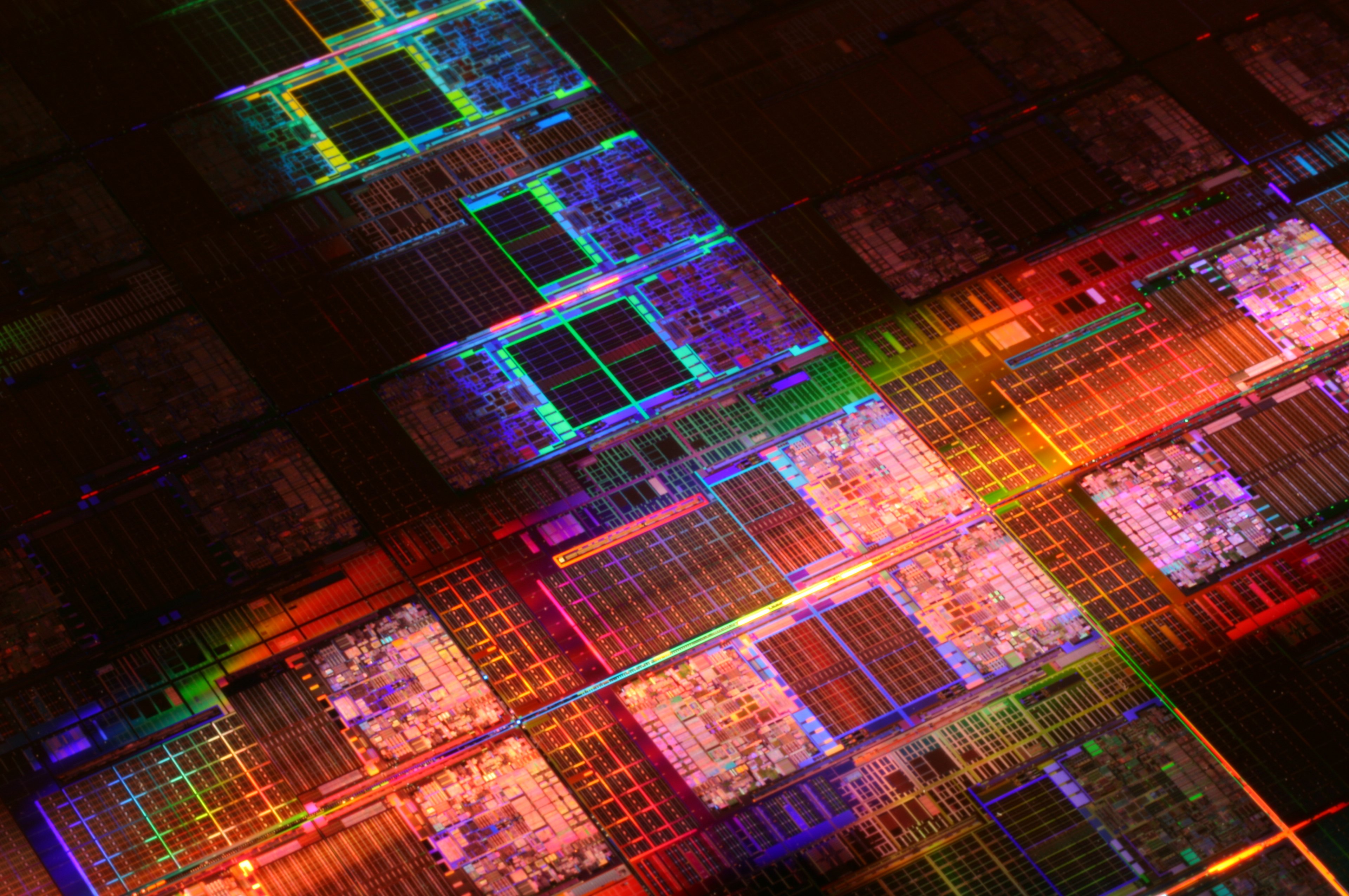
Last week, at the SPIE Photomask Technology + Extreme Ultraviolet Lithography conference, Intel and ASML announced a surprising development. In cooperation with ASML, Intel has already manufactured one million silicon wafers using High-NA, which is a technology representing the next major leap in advanced chip manufacturing after EUV litography. Prior to this, High-NA was expected to be deployed only several years from now.
Intel originally reported that it would deploy High-NA as part of the process it calls 1.4 nm or 14 angstroms (Intel 14A), although of course its results may be somewhat worse than those of TSMC’s 1.4 nm process. Intel has now revealed, however, that it is already using High-NA technology as part of its currently commercially deployed 1.8nm 18A process. The aforementioned one million wafers were not processed solely during the development and prototyping of future technologies, but include regular production batches as well, even though the 18A process was not supposed to use High-NA.
This does not mean, however, that Intel deployed this technology out of desperation because they ran out of other options (think a scenario where the 18A technology could not be made to work without it). Intel confirmed that it uses High-NA to manufacture only a selected portion of its 1.8nm products, while the others are manufactured using the standard process—which therefore has to work without High-NA on its own. This includes some of the Intel Core Ultra 300 “Panther Lake” processors currently shipping in PCs, so we aren’t talking some limited run with an unimportant chip design.
Intel states that High-NA is used to create some selected layers of Panther Lake chips (or rather, their 1.8nm chiplets), with Intel using ASML TWINSCAN EXE:5000 machines or possibly their second-generation TWINSCAN EXE:5200B models—which ones exactly is not entirely clear. Manufacturing with High-NA is technologically more complex, but it allows a single exposure (patterning) to accomplish what conventional EUV would require multiple exposures to achieve. In some cases, this is said to reduce the number of manufacturing steps from 40 to just 10, making manufacturing faster and therefore cheaper. The resolution of the structures that can be created on a chip depends on the resolution that the UV rays used for exposure is capable of achieving. Even EUV (extreme ultraviolet radiation with a wavelength of 13.5 nm) has its limits, however, and creating smaller structures requires combining multiple exposures with overlapping patterns to improve the resolution. High-NA improves the resolution achieved with EUV, so a single exposure patterning can be viable again.
The layers that Intel creates using High-NA machines in this production process, which is simultaneously experimental and proven in regular mass production, would otherwise be manufactured using EUV technology, presumably with multiple exposures to improve the resolution. According to Intel, chips using High-NA have equally good or better parameters compared with those using the conventional process, so it has been demonstrated that the technology can be successfully used.

Intel has already opened up the option of using High-NA EUV as part of the 1.8nm process to Intel Foundry customers as well, i.e. external customers that could manufacture chips in its factories. Intel’s long-term goal is to establish itself in the so-called foundry segment, as it needs greater economies of scale in manufacturing and revenue from other companies in order to remain in the advanced chip manufacturing business against TSMC and other competitors.
What Is High-NA Technology?
High-NA is an extension of current EUV lithography designed to further improve the ability of extreme ultraviolet radiation to form extremely small structures on a chip.
It does this using anamorphic optics with larger mirrors, increasing the numerical aperture from 0.33 to 0.55, which should enable the creation of transistors 1.7× smaller (41% smaller). Implementing this is, of course, more complicated, and there are also disadvantages: this reduction simultaneously halves the area that the High-NA EUV machine patterns on the wafer. Filling the entire wafer therefore requires twice as many exposure steps. It also apparently reduces the maximum chip size, so, for example, large high-end GPUs will necessarily have to become chiplet-based.
An alternative to High-NA is to use double or even multiple EUV exposures, but this means additional manufacturing steps, complicating and increasing the cost of manufacturing. However, multiple patterning can eventually be used with High-NA as well to push chip manufacturing capabilities even further.
The Problem with Large Chips: A Solution on the Horizon?
High-NA technology does, however—or at least for now—have one major disadvantage resulting from the nature of the optical “densification” of the pattern transferred onto the silicon. Today’s processes can manufacture chips with an area of up to around 800 mm² (the maximum size is determined by the so-called “reticle limit”), which is typically used by, for example, Nvidia’s most powerful GPUs. However, as High-NA optically shrinks the pattern formed on the chip, the maximum area that a single chip can occupy is also significantly reduced.
This may not matter at all when manufacturing cheaper processors, mobile SoCs, and mainstream chips, but it would become a problem with powerful GPUs, AI accelerators, or server CPUs, which would necessarily have to switch to a chiplet-based design. Splitting a chip into chiplets is one possible solution to this problem, but even so, the 18A process using High-NA cannot be used for every possible design that Intel or another contract manufacturer might want to produce.
Larger Masks?
This problem could nevertheless have a solution. Current processes use masks for chip exposure that carry the pattern to be transferred onto the silicon and measure 6×6 inches (approximately 150 × 150 mm). A possible solution to the problem of the reduced maximum size of the manufactured chip would therefore be to use larger masks. Intel is investigating and developing this together with ASML, with these larger masks expected to measure 6 × 12 inches (150 × 300 mm).
Using them would once again make it possible to manufacture large monolithic dies, although converting to a new mask format would probably be a complex process with significant costs due to the need to modify mask manufacturing procedures and all the equipment involved. Let’s hope this does not end up like the attempt to reduce manufacturing costs by using larger silicon wafers (450mm wafers instead of 300mm), which fizzled out because converting the large number of factories and individual tools designed to work with 300mm wafers would have been extremely expensive and demanding.

Trailblazing the technology for easier 1.4nm launch?
In any case, this inconspicuous incorporation of High-NA EUV into 18A manufacturing is quite interesting—it is probably not very common for a commercially used technology to receive such an experimental/alternative version involving a significantly modified process. It is possible, however, that this is a remnant of Intel’s earlier plans to apply High-NA to this process as a standard tool. The company may have been developing the process with High-NA from the beginning and kept developing an alternative scheme using conventional EUV technology as a fallback (with more manufacturing steps compensating for its lower resolution). In the end, the version without High-NA was selected for commercial deployment, but based on the original development work, the High-NA variant was now perhaps nevertheless brought to production readiness.
If nothing else, hopefully this will help Intel achieve a smoother ramp-up of the future process in which the technology will be deployed as a standard and no alternative version without High-NA will exist. That is something that should happen with the company’s next, nominally 1.4nm process (Intel 14A) according to the current knowledge of Intel’s plans.
Intel’s competitors are, of course, also testing High-NA manufacturing machines from ASML and using them to develop future processes. It therefore cannot be said that they have less experience with these tools. But such broad deployment in actual production ahead of time could give Intel an advantage when ramping up this technology.
Sources: Intel, techPowerUp
English translation and edit by Jozef Dudáš
⠀