A year ago TSMC introduced 1.6 nm and 1.4 nm chip technologies, which represent—or better said will represent—the most advanced manufacturing nodes for silicon logic circuits that power all modern electronics. Now TSMC has revealed the next milestone: 1.3 nm and 1.2 nm nodes, pushing capabilities even further. Practically all chipmakers and the innovations we’ll see from them in the coming decade depend on TSMC’s technology.
For context—in December, TSMC launched mass production of its 2 nm N2 process (it’s worth reminding that “nanometer numbers” are arbitrary designations and this true not not only with Intel and Samsung, but also with TSMC—they are not directly tied to physical feature sizes). N2 is a completely new generation compared to the 3 nm node and is now the company’s current technology, although we are still waiting for the first chips using it to appear on the market.
Following the 2 nm process, the next new generation will be the 1.4 nm process labeled A14 (as in 14 ångströms, i.e., 1.4 nm). Separately, TSMC is preparing a process labeled 1.6 nm (A16), which is a derivative of the 2 nm process—its improvements come from applying Super Power Rail technology (also known as Backside Power Delivery). These technologies were announced last year; we covered them here:
1.3 nm process (A13)
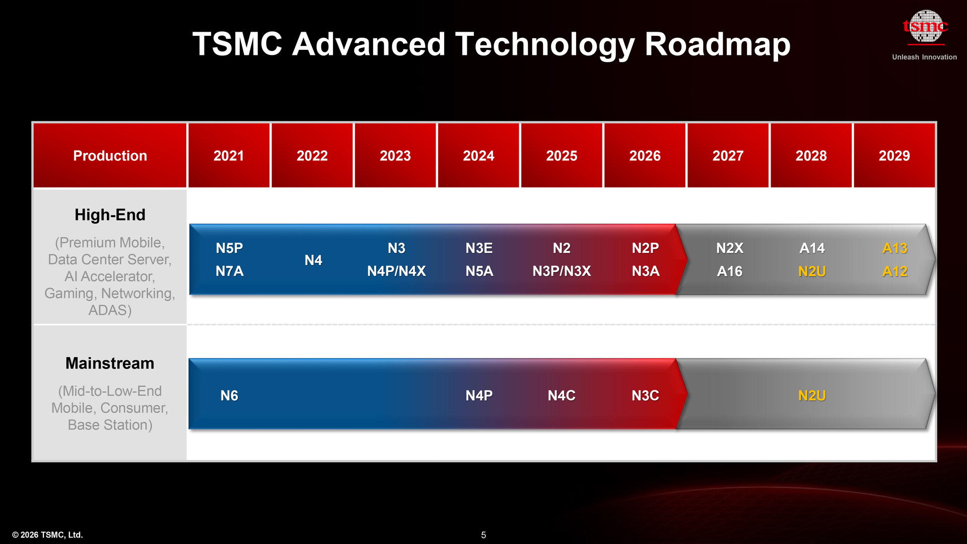
TSMC has now announced the next development that will take over after these: the 1.3 nm A13 process. However, this is not a completely new generation but an evolutionary improvement or optimization of A14—it still belongs to the 1.4 nm family. According to TSMC, A13 will mainly involve “optical shrink” of structures to roughly 97% of the physical size compared to A14.
But this won’t be the only factor; other adjustments will also be involved. The technology will remain electrically compatible and will use the same design rules, so porting chips or IP should require only minor changes rather than a full redesign.
Chips manufactured on the 1.3 nm process will have slightly smaller die area, improving cost per chip—assuming transistor counts don’t increase. TSMC states that transistor density will rise by up to 6% (which is not the same as a 6% area reduction; the area shrink would be about 5.7%, give or take). TSMC has not yet disclosed expected improvements in performance or power consumption.

Production is planned to begin in 2029, roughly a year after the 1.4 nm process (2028). Availability of chips from Apple, AMD, Intel, and others typically comes later, so real‑world products may not appear until 2030. This is the plan, anyway. Delays are always possible—these are extremely demanding technologies, and TSMC is leading the industry, being farthest into the frontiers of silicon technology which also means being the first in the line to face any unexpected obstacles.
1.2 nm process (A12)
TSMC also announced the 1.2 nm process labeled A12 (again implying 12 ångströms, i.e., 1.2 nm). This technology is also not a full-blown new generation succeeding 1.4 nm—the true next generation will likely be labeled A10 (1 nm), but that has not yet been announced.
A12 will still belong to the 1.4 nm family, and like A13, it is an enhancement of A14—in this case, the improvement comes from adopting Super Power Rail (Backside Power Delivery). Thus, A12 will be to A14 what A16 is to N2—a special variant likely used mainly for HPC products.
Using Backside Power Delivery should increase transistor density by moving power rails into separate metal layers. The downside will be higher process complexity and higher manufacturing cost. Besides density, power efficiency and performance should also improve (A12 should reach higher clock speeds). TSMC has not yet disclosed specific expected numbers.
The A12 process is also planned for mass production in 2029, again with commercial availability of resulting products (such as AI GPUs) likely taking several additional months to a year. A12 will probably be used by a smaller set of products, while most customers will rely on A14 and A13 or jump directly to the “next‑gen” A10 node. According to unofficial reports, the A16 process with Backside Power Delivery will be used only by Nvidia for Feynman compute GPUs (AI accelerators), and A12 may similarly be limited to a narrow set of products, though possibly with more clients.
Interestingly, TSMC does not plan to use High‑NA EUV for any of these processes (we explained High-NA technology in this article). At least for now, the company intends to implement these technologies using today’s EUV machines. This simplifies and reduces the cost of development and manufacturing, but there is the risk that should the company overestimated what can be achieved without High‑NA, the technologies may fail to meet planned parameters or encounter issues similar to Intel’s troubled 10 nm process. Intel, incidentally, plans to use High‑NA starting with its 1.4 nm process (Intel 14A).
N2U and N2X: More performance within 2 nm chip generation
Alongside these future technologies, TSMC also announced nearer‑term updates—enhanced versions of the 2 nm N2 process. The company introduced the N2U process, which includes various optimizations combining both the litography‑level and circuit design‑level improvements. Together, these should deliver up to 3–4% higher performance (higher clock speed at a given power level) or 8–10% lower power consumption at the same clock speed compared to N2P. Note: this does not necessarily mean a 3–4% increase in absolute maximum frequency, as these comparisons are usually made at lower points on the voltage‑frequency curve. Transistor density should also improve by 2–3%.
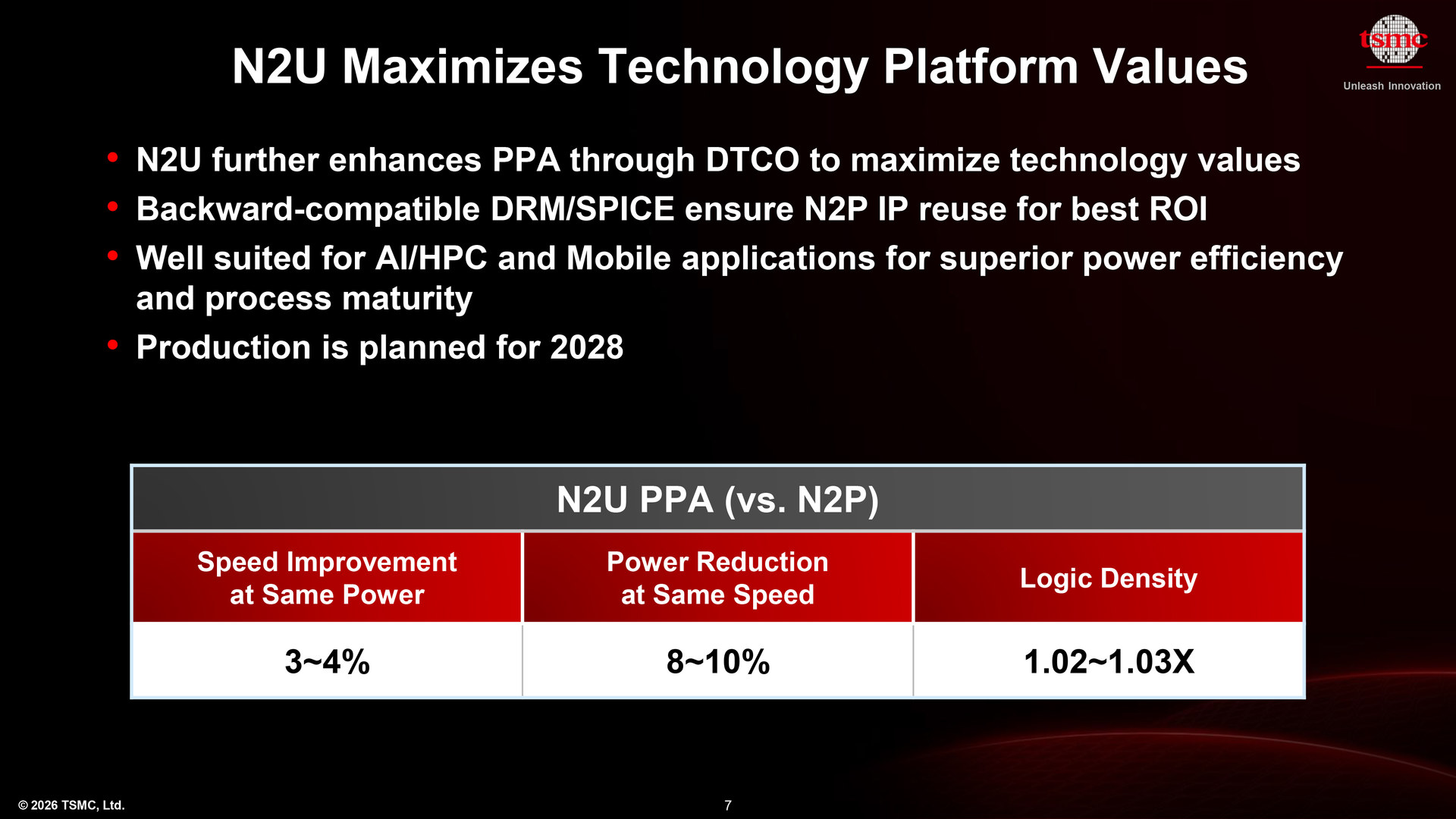
This process should be available in 2028, when mass production is scheduled to begin. It should be suitable for high‑performance GPUs and CPUs as well as mobile SoCs, so it may be what some smartphone chip generations preceding the jump to 1.4 nm will end up using. AMD, Intel, and Nvidia may also use it for some future PC processors and GPUs.
TSMC is also planning the N2X process, which will be even more optimized for high performance, especially for HPC products such as AI GPUs. It should deliver up to 10% higher performance than N2P, or alternatively lower power at the same frequency. N2X may serve similar applications as A16, but free of the additional complexity burden of Backside Power Delivery, making it an alternative for more cautious customers. Both processes are scheduled to begin production in 2027.
Source: Tom’s Hardware
English translation and edit by Jozef Dudáš
⠀