
Nvidia had their GTC 2022 keynote scheduled for Tuesday. As expected, company CEO Jen-Hsun Huang finally unveiled new gaming graphics cards at this presentation alongside various enterprise, AI, and automotive stuff: the GeForce RTX 4090 and GeForce RTX 4080 with the new Ada Lovelace architecture. They’ll come to market in the next two months, however we don’t exactly have good news on the prices Nvidia will charge for them.
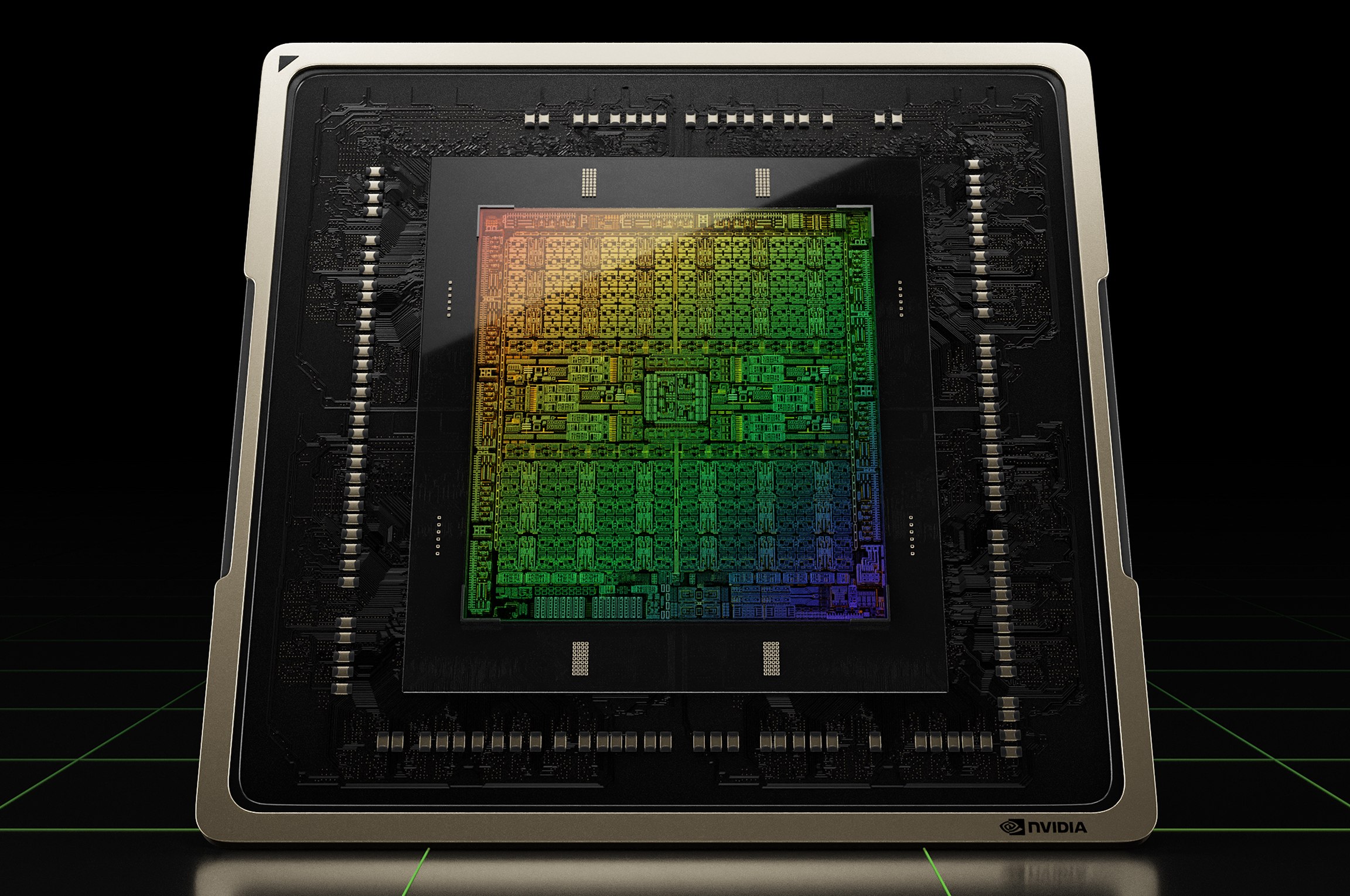
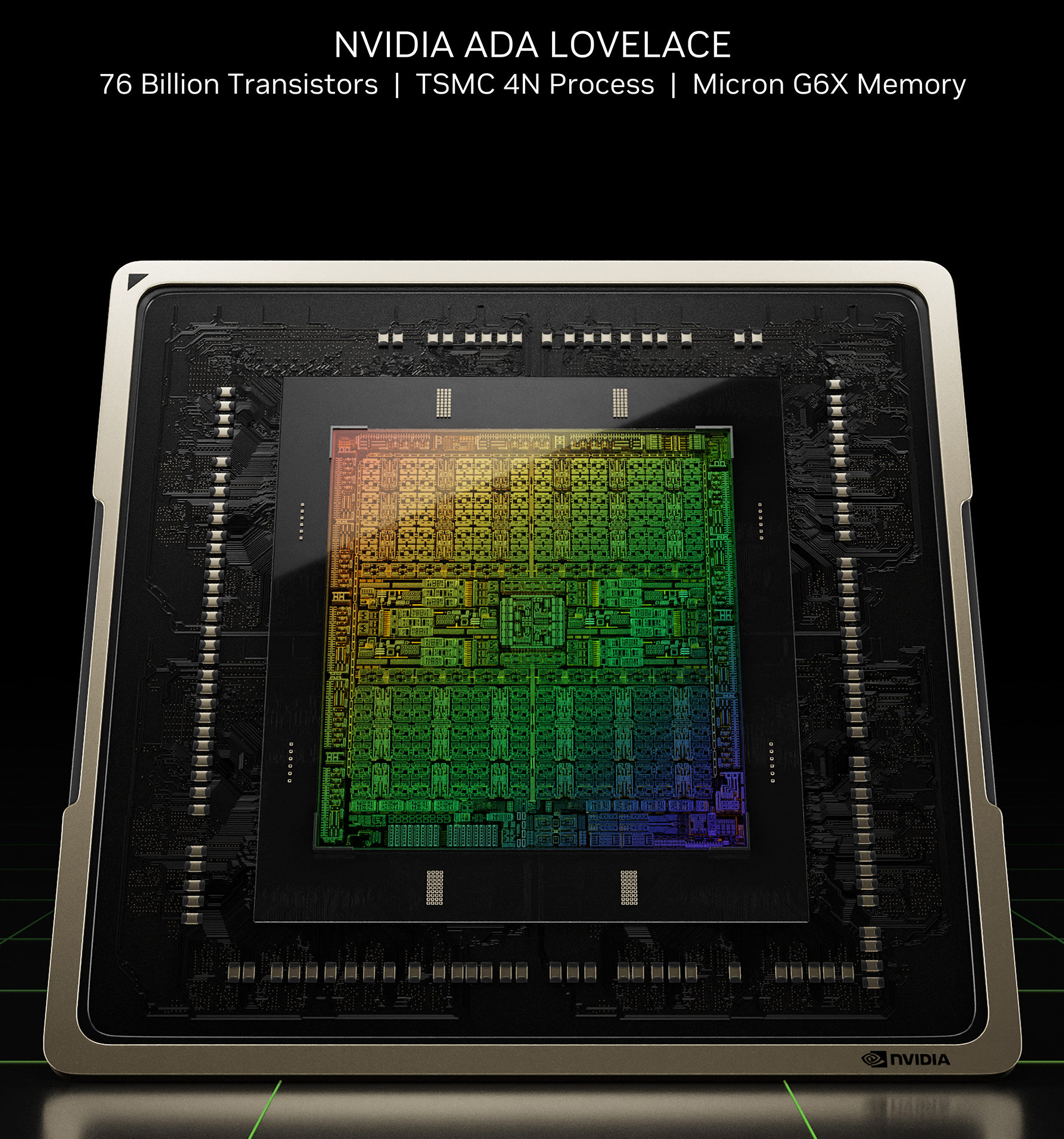
GeForce RTX 4000 is a new generation of GPUs and a new architecture. It’s named after an early programming pioneer and we have been referring to it as Lovelace in the past. However, it seems that while the full name is “Ada Lovelace”, Nvidia people are now mostly using the shortened name Ada. Either way, it’s the same architecture, the unofficial leaks weren’t wrong about the naming. Nvidia uses the 4N process to manufacture Ada Lovelace chips, which is a modified version of TSMC’s 4nm process (or 5nm according to some unofficial sources, however the modifications may be so far-reaching that it deserves the 4nm designation anyway).
Ada (Lovelace): New shaders, RT cores and Tensor cores
The architecture brings a new generation of SM blocks containing shaders (FP32 units), a fourth generation of Tensor cores with support for FP8 computing (this is apparently the same architecture as in the Hopper GPU) and a third generation of RT cores for ray tracing.
These are said to have up to 2× the computational performance available for finding intersections of rays with triangles. Third-generation RT cores also have new OMM (Opacity Micromap) and DMM (Displaced Micro-Mesh) engines. The former speeds up ray tracing calculations dealing with transparent textures and objects, while the latter speeds up BVH structure building (BVH is an auxiliary box system wrapping around 3D structures used as a helper in ray intersection analysis) for scenes with complex geometry.
Ada probably involves a large number of different changes under the surface (the GPUs, by the way, support CUDA 8.9, while Ampere supports just CUDA 8.6), but Nvidia has so far limited its presentation to revealing one important architectural change: Shader Execution Reordering (SER).
Presumably this would be some form of ability to dynamically change the scheduling of shaders to individual SM units, and re-order their execution to make optimal use of GPU resources. So it could be some sort of Out-of-Order instruction execution on CPUs. This technique is supposed to significantly improve the performance extractable from shaders (FP32 units).
In this first wave, Nvidia announced two, or technically three next-generation graphics card models:
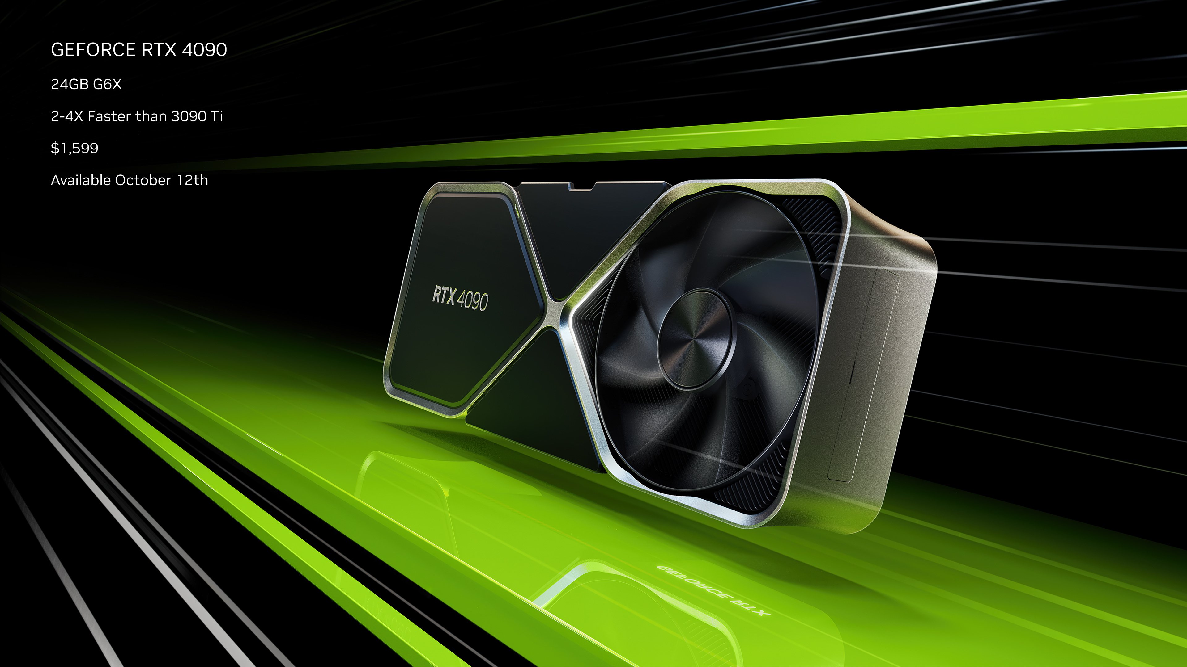
GeForce RTX 4090
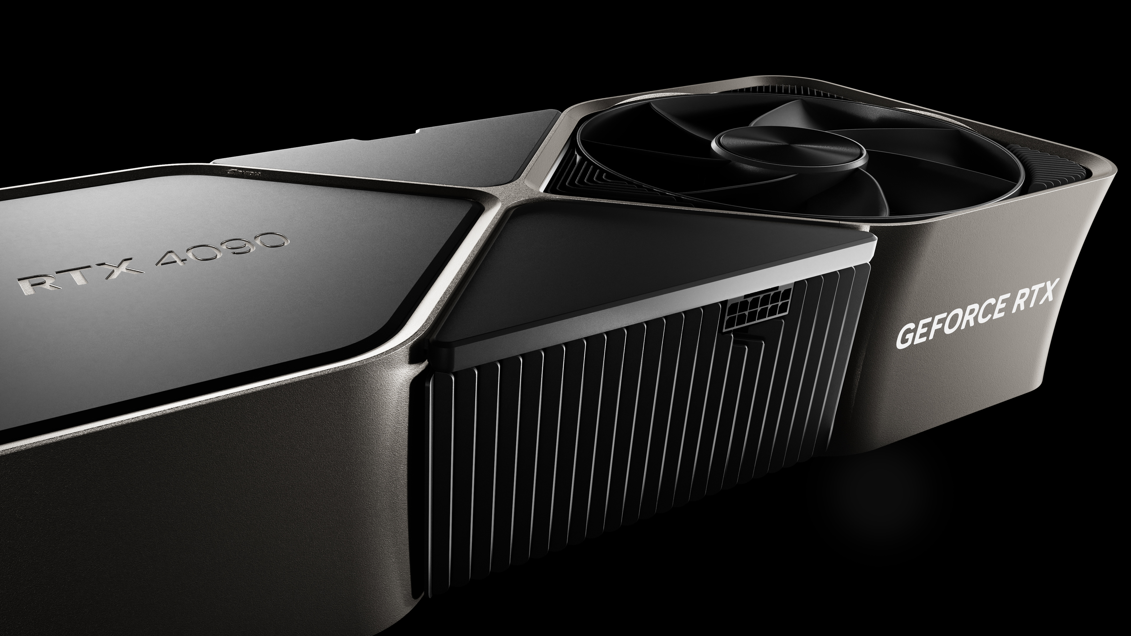
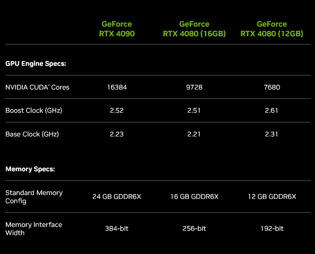
The top of the lineup is the GeForce RTX 4090, which is supposed to be based on Ada Lovelace’s largest GPU of the generation, the AD102. However, it doesn’t have its full configuration. According to Nvidia, the AD102 chip contains 76.3 billion transistors and over 18,000 FP32 units (it should be 144 SM blocks, so exact number is 18,432 shaders, 576 Tensor cores and 144 RT cores). It can produce up to 90 TFLOPS of performance in FP32 operations with them. The die area is 608.4 mm².
In the GeForce RTX 4090, however, this chip is trimmed down to 16,384 shaders (128 SM blocks) and is claimed to have a theoretical performance of “merely” 83 TFLOPS. Its base clock speed is 2.23 GHz and the boost is 2.52 GHz, while realistically the GPU will probably run higher. According to Nvidia, they managed to overclock an Ada GPU above 3.0 GHz “in the lab”, but we don’t know if they are talking about the AD102 chip and if it was a practical day-to-day overclock and not some LN2 stunt.
The card uses the full 384-bit bus of the AD102 chip and carries 24 GB of GDDR6X memory, which should have a clock speed of 21.0 GHz (effective), and thus a bandwidth of 1008 GB/s. The GPU has 72MB L2 cache and 176 ROPs enabled.
These graphics will have a default TDP of 450 W like the GeForce RTX 3090 Ti (but OC cards can probably have it increased). According to Nvidia, this card is up to 2–4× faster than that Ampere SKU, however, the four times figure is probably valid for some selected atypical case, the 2× figure is more likely to be closer to typical performance. As usual though, remember that these are official benchmark results, which may be selective or otherwise manipulated. Therefore, it is better to wait for independent reviews before drawing conclusions.
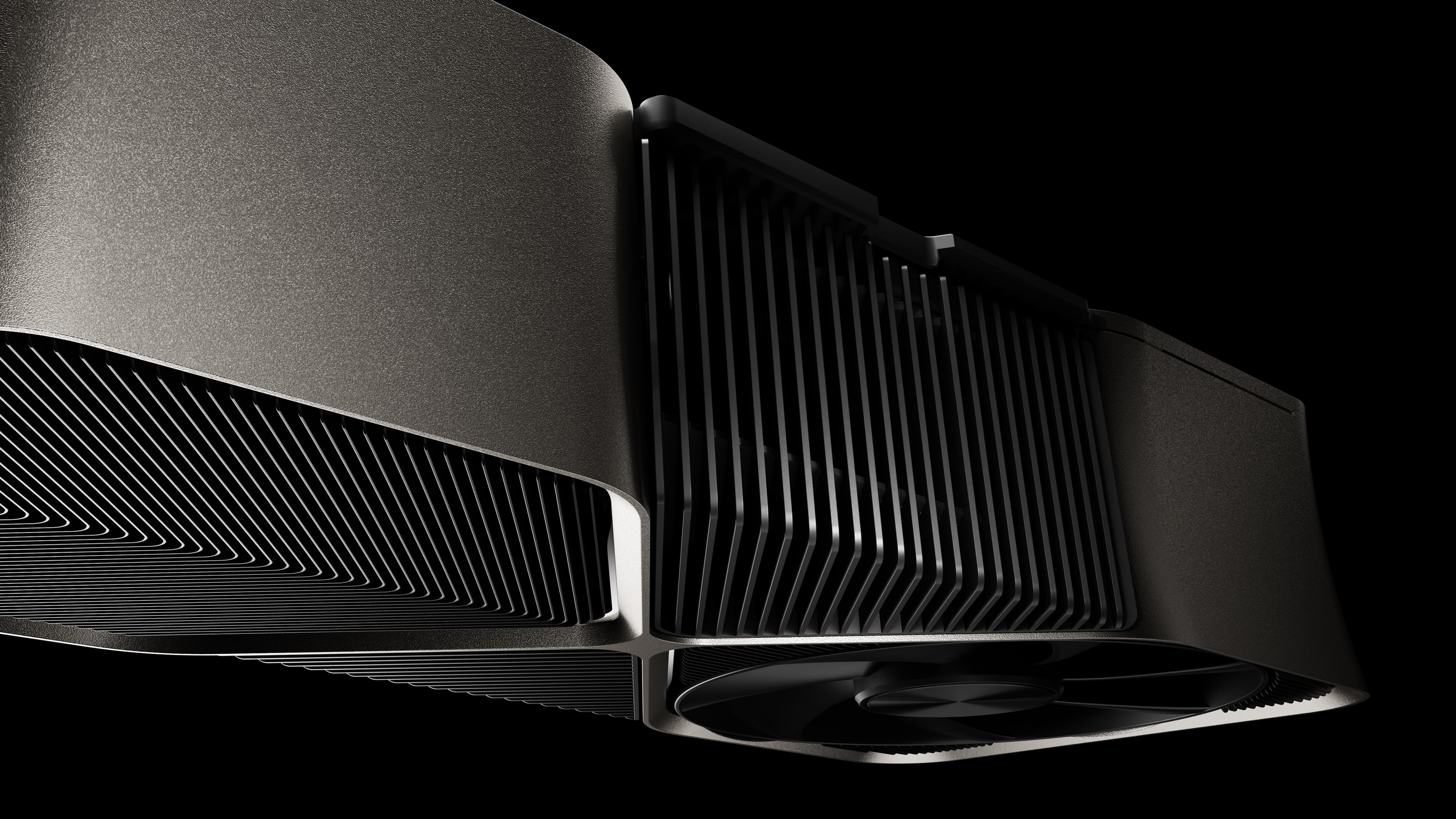
Those aren’t that far off, because according to Nvidia, the GeForce RTX 4090 will be released on Oct. 12, three weeks from now. The card will be offered in non-reference versions from various manufacturers, as well as a Founders Edition directly from Nvidia, which you can see in the images. It’s a three-slot card with the same cooling design as the RTX 3090 and 3090 Ti have, but the fans are bigger.
The RTX 4090 uses a 16-pin ATX 3.0 / 12VHPWR power supply connector that must deliver at least 450 W. Optionally, however, it is possible to use an adapter to three classic eight-pin connectors. 850 W power supply or higher is recommended.
Read more: 660 W power draw a reality? Non-reference GeForce RTX 4090 card has a four-slot cooler, 13 heatpipes
What you aren’t going to like is the price. Jen-Hsun Huang announced that you’ll pay 1599 USD for this model in the reference version, even more than the previous Ampere generation’s top card (RTX 3090) used to cost at launch. In Europe, that now comes out to 1941 EUR with VAT.
GeForce RTX 4080 16GB
Nvidia announced the second model in the line too, but as previously leaked, it’s actually two models. The better one of these cards is the “GeForce RTX 4080 16GB”. It hasn’t been said officially, but it’s apparently based on another chip, the AD103. Here again, Nvidia claims a similar 2–4× increase in performance, but this time it’s against the GeForce RTX 3080 Ti. And again, you can probably count on the the lower side of that range being representative of the typical cases.
This 16 GB version of the GeForce RTX 4080 has 9728 shaders (76 SMs) running at a similar clock speed to the higher model – officially 2.21 GHz base and 2.505 GHz boost.
This card has a 256-bit memory bus with 16 GB of GDDR6X memory. But according to unofficial information, it’s already clocked at 22.4 GHz (effective), giving it a bandwidth of 716 GB/s (that’s over 90 % of the bandwidth of the GeForce RTX 3080 10GB). There’s 72 MB of L2 cache and 112 ROP units in the GPU.
The TDP of this card is said to be 320 W, and it also requires a power supply with either a 450 W ATX 3.0 16pin or a three eight-pins via adapter.
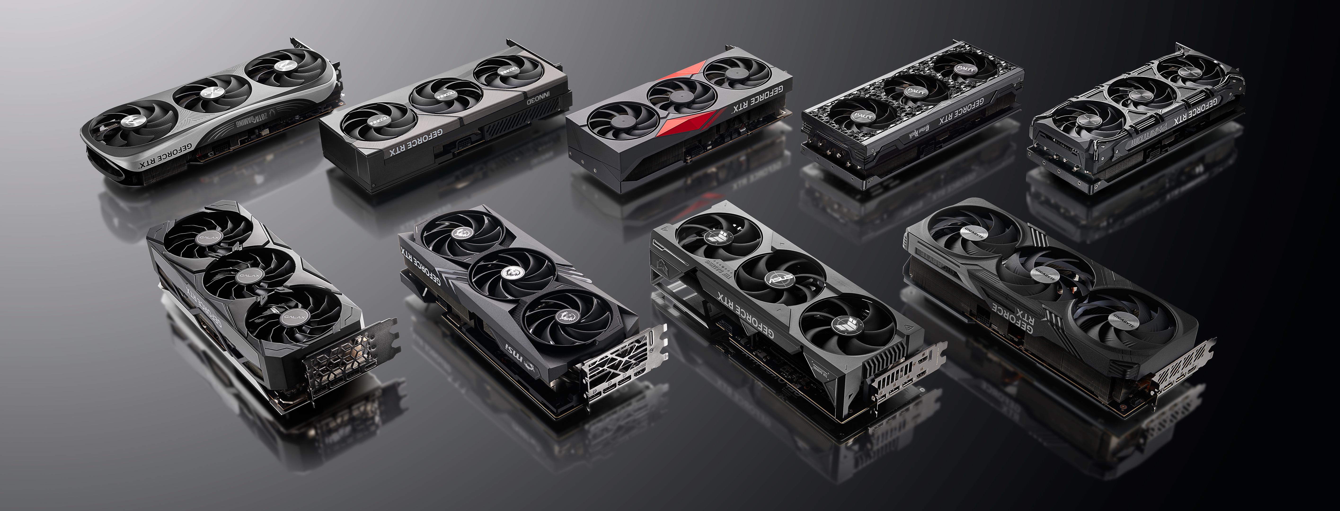
This card will also be available in both non-reference and reference Founders Edition versions (those have a similar three-slot cooler as RTX 4090). This card will come out later, it is supposed to go on sale in November. Nvidia has set the price at 1199 USD, which currently means 1456 EUR including VAT in Europe. AS a reminder: two years ago the equivalent of this card (RTX 3080) had a recommended price of 699 USD. That’s a 71.5 % increase in price…

GeForce RTX 4070 RTX 4080 12GB
But Nvidia will also offer a GeForce RTX 4080 card with 12 GB of GDDR6X memory. However, it’s so different enough that it should probably be called the RTX 4070, and in fact it’s really closer to being a third model in the lineup (which two years ago was the RTX 3070 and four years ago the RTX 2070). It’s even allegedly based on a different chip, the AD104 (RTX 3070 was based on GA104, by the way).
The GeForce RTX 4080 12GB has only 7680 shaders (60 SMs). Its clock speeds are about 100 MHz higher (base 2.31 GHz, boost 2.61 GHz), but that doesn’t make up for the large reduction in compute units. There is also the problem that not only memory capacity is reduced, but also bandwidth. The GPU only has a 192-bit bus and GDDR6X memory on it with an effective clock speed of 21.0 GHz, giving a bandwidth of just 504 GB/s. There’s 48 MB of L2 cache and 80 ROP units in the GPU.
The TDP of this card is 285 W and its power supply is either 16-pin (but it is only required to supply 300 W in this case) or an adapter for two classic eight-pins. This card may not have a Founders Edition version, but only non-reference cards. Its release will also apparently not be until November.
Performance will be significantly lower than the RTX 4080 16GB due to the specs, probably roughly matching the position that the RTX 4070 would normally have. So why didn’t Nvidia use this name? Perhaps because this card will also have a shockingly high price tag – the company will ask for 899 USD. That price is 80 % higher than what the GeForce RTX 3070 officially costs, so the higher-numbered designation is probably an attempt to make the price bump look more acceptable. For us in Europe, the recommended sum after VAT at current exchange rates corresponds to 1092 EUR.
Cheaper graphics cards still only RTX 3000
The rest of the lineup has not yet been announced and will probably not come until next year. Nvidia even made it explicit in the presentation that it will continue to sell a portion of the Ampere generation GPUs – the GeForce RTX 3080, RTX 3070, and RTX 3060 models – below the three new Ada graphics.
The speculation looms as to whether Nvidia perhaps priced both GeForce RTX 4080 models so brutally to leave room for continued sales of these Ampere generation GPUs without having to significantly slash their prices. Who knows, perhaps Nvidia might yet be forced to cheapen the new cards in he future due to competitive pressure from AMD, which will launch its own next-generation GPUs in about two months as well. But there’s chance AMD may simply deploy higher prices as well, instead.
BTW: leaker Kopite7kimi, who has very good internal sources, says that even the price of the RTX 4090 may have originally been aiming higher, he says it was only revised to 1599 USD fairly shortly before the actual presentation went public. At least, that’s according to his sources, but this is a hard-to-verify claim (unless the non-final slides showing the original price leak one day).
Connectivity and multimedia features: without DisplayPort 2.0 and only with PCIe 4.0, but with AV1 encoders
GPUs of the Ada Lovelace architecture, on the other hand, don’t bring some of the new features you might have been expecting. For example, they still stick to PCI Express 4.0 ×16 interface, so these GPUs don’t use PCI Express 5.0 to connect to the system. This isn’t necessarily a big flaw, as it’s possible that the double bandwidth of the new generation PCIe lanes wouldn’t bring any real performance gains. Nvidia has also removed NVLink and SLI support completely, even the top of the line RTX 4090 doesn’t have it anymore.
What is also unchanged is apparently the DisplayPort output. According to specs, Ada Lovelace can only provide DisplayPort 1.4a for now, and not DisplayPort 2.0, but even so, resolutions up to 7680×4320 pixels are supported, including 12-bit HDR at 60Hz. 4K resolution is possible at up to 240 Hz, but both these configurations require DSC compression. HDMI 2.1a outputs support 4K at 120 Hz and 8K at 60 Hz, including HDR.
The hardware video decoders are also seemingly unchanged from Ampere, Nvidia uses the same 5th generation decoder block, however that block already supports more or less all relevant formats up to AV1 (only the VVC format is not supported).
But more importantly, Ada Lovelace introduces a new 8th generation encoder (compression) block, while Ampere and Turing have 7th generation block. To be more precise, there are two parallel encoders on both the GeForce RTX 4080 and RTX 4090. This new generation could achieve better encoded video quality, but in particular, it brings support for encoding to the AV1 video format for the first time. First time in Nvidia GPU that is, it’s not a world’s first implementation. That victory was achieved by Intel with its Arc GPUs.
Sources: Nvidia (1, 2, 3), VideoCardz (1, 2)
English translation and edit by Jozef Dudáš
⠀