While we wait for the refresh of Arrow Lake desktop CPUs—except the cancelled the top-tier SKU—new details have surfaced shedding light on the upcoming Core Ultra 400 “Nova Lake” generation, expected to deliver a major next-gen leap. The leaks cover power consumption and cooling, as well as the architecture of the high-performance cores in these processors. Intel is preparing a previously unseen change to CPU cache and interconnect design.
We’ve known for some time that Nova Lake will come in a version featuring two compute chiplets—similar in concept to AMD’s Ryzen 9 models with dual CPU core dies. This configuration will include two clusters of 8 P-Cores and 16 E-Cores. In addition, there will be four low-power LP E-Cores in the SoC tile, bringing the total to either 25 or 48+4 cores.
However, this version will apparently come with substantial power demands under load. According to leaker Kopite7kimi—best known for Nvidia GPU disclosures—52-core configurations could reportedly reach up to 700 W if power limits are unlocked, which aligns with estimates from one of the most reliable sources on upcoming Intel silicon, the leaker known as Jaykihn.
Jaykihn cautions that this is not an official power configuration. Meanwhile, a table outlining various power limits appeared online too, but according to them it is already outdated and was something that applied to an earlier sample with fewer cores—14 P-Cores and 24 E-Cores.
At present, Jaykihn states that Intel is targeting a “maximum turbo power” (PL2 limit) of 400 W for the 52-core model. A non-overclocked processor should therefore not exceed this figure, and under full multi-core load, power draw should remain at or below this level. Intel has thus opted for a still relatively conservative figure—current 8+16-core Intel processors ship with a default maximum turbo power of 253 W, meaning a roughly 60% increase for chips with double the core count. That said, so-called extreme profiles may exist that push the limit higher. The 400 W figure—or possibly “400 W+,” hinting at potential upward adjustment—corresponds to a performance profile, not an extreme one, but also not the reduced “baseline profile” intended for cheaper, less robust motherboards.
This PL2 value remains provisional, meaning Intel could still raise it before specifications are finalized. Officially stated TDP is expected to be 175 W for dual-chiplet models (unlocked single-chiplet SKUs will likely remain at 125 W TDP, though this is speculative).
TDP does not represent typical power consumption but rather something closer to the minimum cooling capacity required for the processor to operate at nominal specifications. However, if your cooling solution can dissipate only 175 W rather than the full 400 W, the CPU will not deliver full performance under multi-threaded workloads. It will reach maximum temperature and begin throttling. In single-threaded loads, we expect that the power use will most likely fall somewhere between 40 and 60 W.
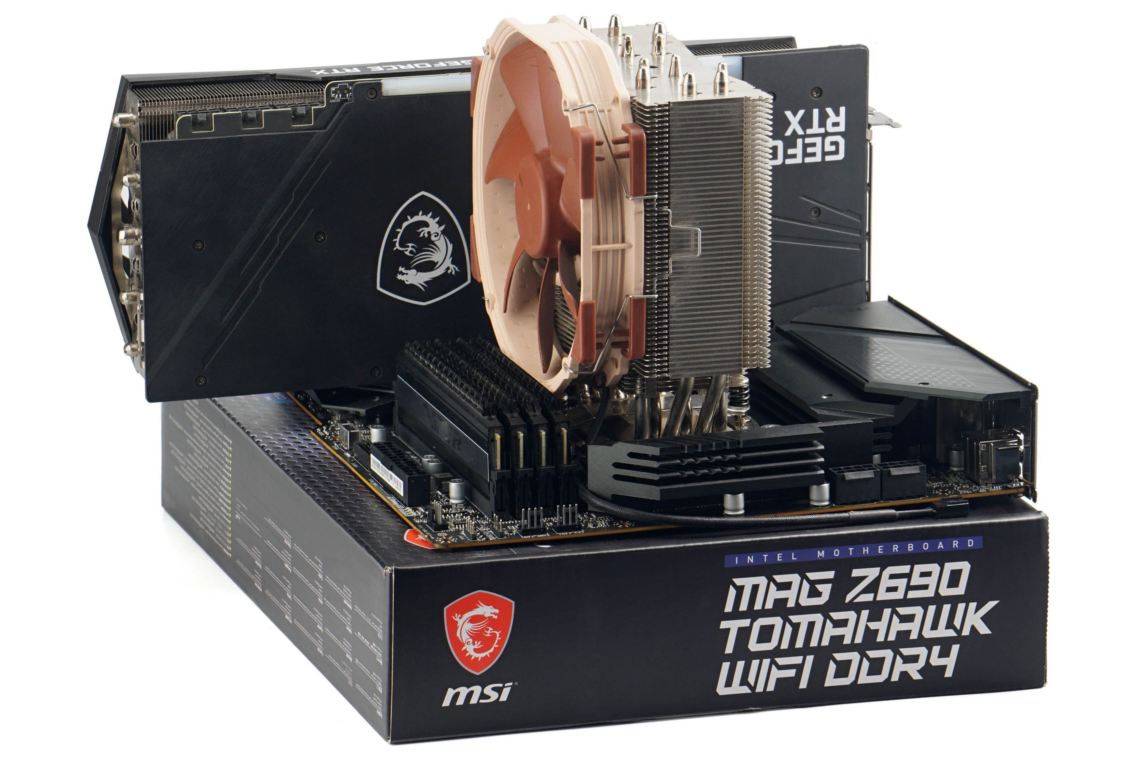
Incidentally, according to Jaykihn, the Noctua U14S cooler should be capable of handling a 52-core Nova Lake processor with a 400 W PL2—but not at full performance. The long-term sustainable power level with this cooler is said to be around 307 W, which would mean sustained clocks would be reduced accordingly.
52 cores only for select enthusiast motherboards?
Although the dual-chiplet processor version will use the same LGA 1954 socket as standard single-chiplet CPUs (which will top out at 8 P-Cores, 16 E-Cores, and 4 LP E-Cores), it may not be supported on all boards.
Jaykihn reports that, according to his information—which remains preliminary—some LGA 1954 motherboards may be limited to lower-tier single-chiplet processors only. Others may support dual-chiplet CPUs but with reduced performance, likely via something akin to a “baseline profile,” where PL2 will be capped below the 400 W performance profile figure.
VideoCardz chimed in that dual-chiplet processors could effectively serve as a replacement for the HEDT platform. They would likely be paired with select high-end—and presumably expensive—motherboards, and could potentially carry branding such as Core Ultra X9 490X.
The reason not all boards will support dual-CPU-chiplet models is straightforward. A processor with twice the core count will draw significantly more current, requiring motherboards with more VRM phases. The necessary components and PCB real estate may demand a substantial bill of materials—likely prohibitive for many lower-cost boards.
It’s also worth noting that even if PL2 was capped at, say, roughly 250 W instead of 400 W—as is typical on LGA 1851 platform—that would not necessarily translate to a proportionally lower current requirement. Reducing power and frequency also lowers voltage, meaning current drops less than linearly (power equals current times voltage). And for stressing od the VRMs, what matters is current (amperage)—not watts. The power delivery subsystem must also handle transient spikes that jump significantly above average draw—and with 52 cores, those spikes could be considerable.

Nova Lake shifts to a clustered P-Core architecture
Another previously rumored but now substantiated detail concerns a significant change in how cores are interconnected within the CPU. Since the 2008 Nehalem, Intel’s high-performance cores have featured private L2 caches and individual connections to the CPU interconnect—since Sandy Bridge in 2011, this has taken the form of a ring bus topology. When Intel introduced hybrid processors, E-Cores were integrated differently. They are organized into clusters—typically groups of four cores—sharing a common L2 cache, with the entire cluster connected to the ring bus via a single shared stop/node.
With Nova Lake, Intel will for the first time also group P-Cores into clusters sharing a common L2 cache. Each cluster will likely behave similarly to an E-Core cluster and connect to the ring via a single node. However, P-Core clusters will consist of two cores rather than four. The capacity of their shared L2 cache is not yet known. Current E-Core clusters feature 4 MB of L2, while today’s P-Cores have private 3 MB or 2.5 MB L2 caches.
The precise performance implications remain unclear. On one hand, having two high-performance cores share a single interconnect interface cold introduce a potential bottleneck. On the other hand, if Intel ensures sufficient bandwidth toward L3 cache and memory while handling contention efficiently, this architecture could bring benefits. A shared L2 may allow for increased capacity, and in lightly threaded scenarios, a single active thread could leverage the full L2 capacity intended for two cores.
Additionally, reducing the number of ring bus stops used by P-Cores from eight to four should improve interconnect performance, as ring bus efficiency declines with increasing length. The clustered P-Core design could therefore improve internal communication latencies, including L3 latency and overall performance. What may appear to be a minor architectural tweak could thus meaningfully enhance CPU efficiency. Intel has hopefully used the past several generations to refine clustered L2 cache design with E-Cores, so the implementation in P-Cores may already be well optimized.
According to Jaykihn, Nova Lake will also support disabling entire core clusters—meaning individual cores within a cluster likely cannot be turned off independently. The processor should be capable of running with only E-Cores and LP E-Cores active—or even exclusively LP E-Cores.
Thermal throttling disable option to be removed
The information also indicates that users will not be able to modify the TJMax, maximum permitted junction temperature (se to 100°C), nor will it be possible to manually disable thermal throttling. This is likely a response to the misuse of these controls for “performance tuning”—a practice Intel quietly tolerated and at times may have even encouraged—which contributed to stability and degradation issues with Raptor Lake processors. Intel appears set to enforce stricter adherence to official specifications going forward.
Sources: Kopite7kimi (1, 2), Jaykihn (1, 2, 3, 4, 5, 6, 7), VideoCardz
English translation and edit by Jozef Dudáš
⠀