


After Intel, AMD has now presented its new products. These include the Ryzen 5000G APU, Radeon RX 6000M graphics for laptops and FSR upscaling intended as a competition for DLSS from Nvidia. But the processor news was the most interesting thing: 3D silicon chiplets layered on top of each other may come into Ryzen processors, and AMD has shown a prototype, which has 3× larger L3 cache, bringing nice gaming performance boosts.
The first processor news at Computex was about desktop APUs, but we will look at that in another article. The second news is much more surprising and interesting. At the very end of the keynote AMD’s CEO Lisa Su revealed a processor technology with 3D packaging of active chiplets. This is something that has not been seen in a desktop CPU yet.
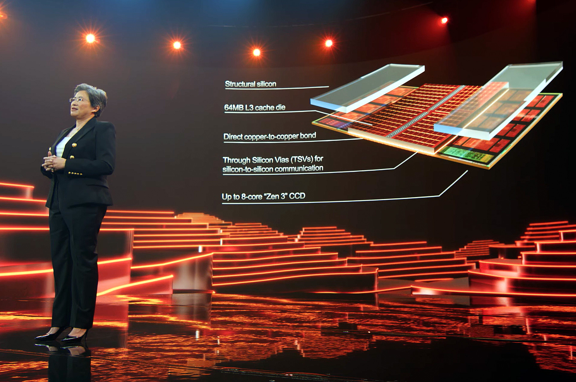
Active 3D chiplets means that two active silicon modules are layered and interconnected by contacts. Su revealed that AMD (apparently in partnership with TSMC, likely using its Chip-on-Wafer tech) had developed technology that would allow it to stack a second chip on top of the CPU chiplet in Epyc or Ryzen processors. What’s more, they have even successfully demonstrated it now.
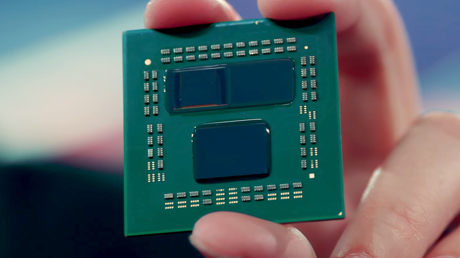
It’s supposed to work with Ryzen 5000 chiplets, whose design had likely been designed to accommodate this technology from the start, because Lisa Su has showed a prototype, which consisted of a Ryzen 9 5900X with an added chiplet. The delidded sample, which you can see in screenshots from the webcast, has a second layer of silicon stacked only on the right of its two CPU chiplets to allow easy comparison, but the functional prototype has both of course (and the whole thing is covered and protected by the heatspreader).
3D Vertical Cache
The role of the second layer of silicon in this phase of the technology is to add extra L3 cache, the so-called 3D Vertical Cache (3D V-Cache). It is a chiplet consisting of SRAM memory and some control logic, which is stacked on the CPU chiplet. The CPU chiplet must first be drilled through to form channels (so-called TSV) with a conductive copper path, because the circuits of the CPU chiplet are on its underside. The contacts of the second added silicon layer are connected to these channels and everything is fixed together.
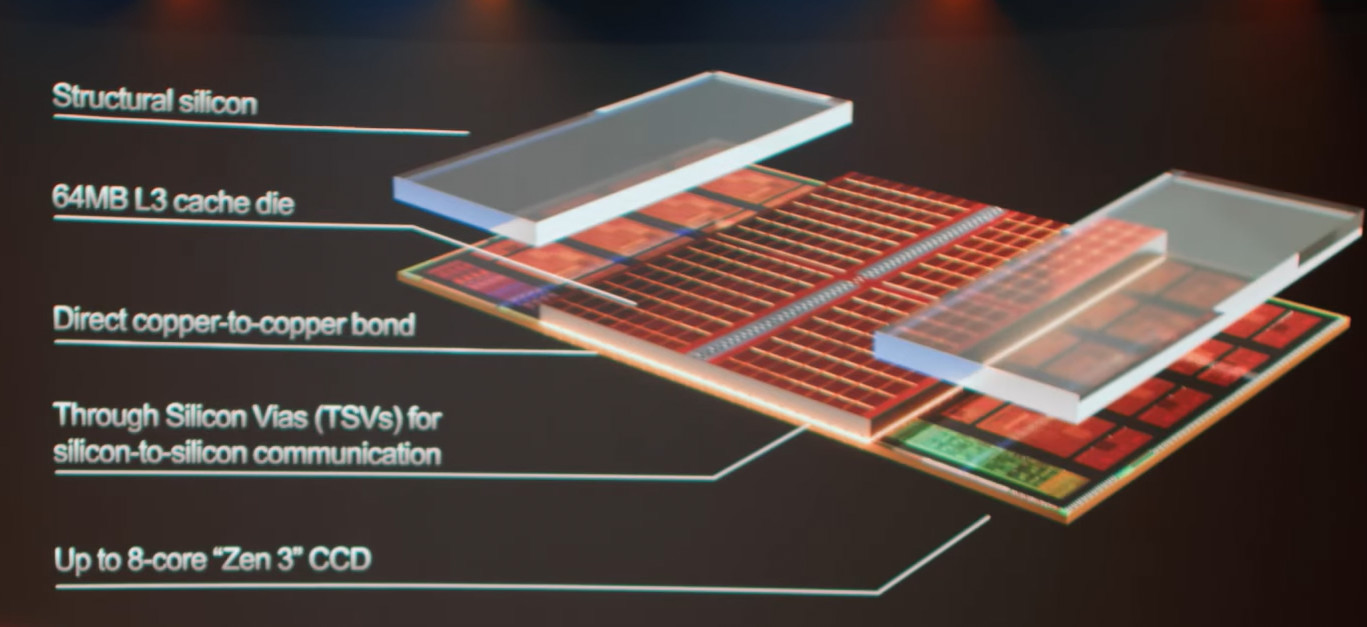
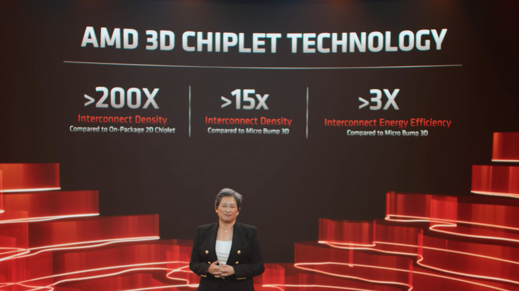
The second chiplet adds 64 MB of cache to a single CPU chiplet (with eight cores), so a single-chiplet processor thus enhanced would have 96 MB of L3 cache (64 MB plus the already present 32 MB), but a model with 12 or 16 cores already will end up with 192 MB (2 × 96 MB). The bandwidth to this cache is reportedly 2 TB/s and this technology is said to have the best energy efficiency in the world. It does not use solder bumps at all, instead the chiplet’s copper contacts directly bonded with the copper channels in the TSVs. This is said to improve the energy efficiency of the connection by the factor of 3× compared to competing technologies that rely on micro bumps.
In addition, the chip with cache is also said to be made on a 7nm process and has an area of approx. 6 × 6 mm (36 mm²). This is interesting because it seems to have a higher density than the L3 cache on CPU chiplets. It is probably made with higher density libraries. We would quite like to know if SRAM on this chip achieves the same performance and what the latency is like. It would probably not be strange if the blocks on the secondary chip had a higher latency than the locally present part of the cache. But AMD does not refer to this additional capacity as L4 and explicitly calls it L3 cache, which implies that it is on the same level as the integrated 32MB cache block.
Obří cache pomáhá ve hrách
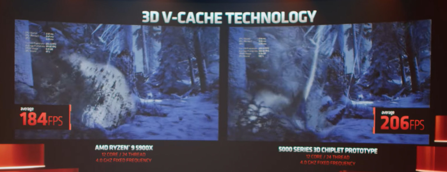
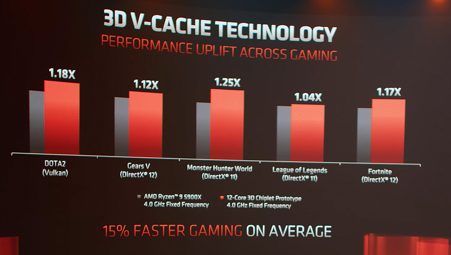
Samples seem to already exist as AMD showed a video with a recorded demo of 3D V-cache in Gears 5. The video compared two 12-core Ryzen 5900X CPUs at the same clock rate (fixed to 4.0 GHz), one of which had 192MB of 3D V-Cache and on average, it achieved a 12% better frame rate. In other games, the increases were even higher (Monster Hunter World on DX11 reportedly gains +25% FPS), so on average it yields about a 15% FPS improvement in games.
So, this technology could improve gaming performance, and quite possibly could be a response to Intel’s advances in IPC promised by the upcoming Alder Lake processors (with up to 20% improvement in single-threaded performance).
To appear in Ryzen as well?
But we do not know whether this technology will really be dispatched to ward off Alder Lake, it is only a prototype so far. AMD states that according to its plan, the company will be ready to start production of such processors by the end of this year. This all but guarantees that the launch can happen in 2022 at the earliest, perhaps a few months after the year’s start. Although the Zen 3 chiplets appear to be prepared for the TSV skewering (which is and interesting discovery, since this must have slightly degraded the die’s transistor density) and for utilizing the 3D V-cache, this may not actually be productised during their lifetime. AMD may deploy this commercially only later, for example with the Ryzen 7000, 8000…
… or perhaps not at all. As usual with advanced technologies, things like HBM2, silicon interposers, and perhaps even this, are often so expensive that they are only deployed in enterprise and server products. According to various leaks, AMD is actually preparing a version of Epyc 7003 processors with such an extended cache (64-core model would have a total of 768 MB L3 cache, 8 × 96 MB!), which is said to be codenamed Milan-X. So it will likely appear in the hands of some enterprise users with deep pockets next year, perhaps in supercomputers. Whether it will appear in Ryzen products is not so clear. Later, there should probably be such a version of processors with Zen 4 cores, Epyc „Genoa-X“.
What could give us hope is if the 3D V-Cache were assembled together with CPU chiplets before being packaged onto the substrate of the entire CPU. If the manufacturing flow was like that, it would not be so expensive to divert some of such assembled chiplet stacks to select premium versions of Ryzen 5000 (or 6000 and so on). But better not get your hopes too high yet. It would be a highly interesting CPU if it worked out, but I’m a little afraid that it’s in “too good to be true” area, even though AMD actually did chose a Ryzen for a demo now. The reason for that may just be that experimenting on a small AM4 processor with one or two chiplets is easier. However, we will be on the lookout for leaks about this technology coming to regular PC users.

Cooling might be an issue… and the price
This technology offers quite a lot of possibilities, especially if the second circuit was not limited to being just cache, or if it would be possible to stack more of them in the future. The second layer could also be logic circuit and act as a chipset—Intel already does this using Foveros technology in Lakefield processors, where the CPU chiplet is on the top and the chipset chiplet on the bottom. This is a slightly different technology, but you can probably say that Intel was first, although it has not yet used this layering method in a very interesting product (which, of course, is probably a fault of poor quality 10nm process used in Lakefield — the next try will be with 7nm Meteor Lake, where the result could be on a wholy different level).
However, the fact this has been announced by AMD comes as a surprise. The company has favored cheap conventional packaging technologies for processors so far, instead of using a silicon interposer for Epyc, for example, to improve performance and energy efficiency. Foveros is also said to use solder for the contacts by the way, which, as already said, is less efficient (density is lower and the interface consumes more energy) than TSMC’s Chip-on-Wafer technology that will be used by AMD.
On the one hand, the weak point is going to be the cost—this will not be cheap at all, so if you are now itching to get your 3D V-Cache CPU, you might want to temper your expectations, because it is quite possible that when the thing comes to market, you will not find it reasonably priced. The second problem is power consumption—or rather cooling. The chiplet on the top, even if it has low power draw itself, probably might have adverse effects on cooling of the bottom chiplet, which in the case of 3D Vertical Cache will probably be what generates most of the heat. When transfering the heat to the heat spreader and cooler, it will first have to pass through the attached second chiplet, which will probably slow down its dissipation and the temperature of the CPU chiplet will be worse as a result, with the equipped cooler being identical. At the same time, the small chiplets in Ryzen are already rather hard-to-cool due to their small surface, and that could get somewhat more pronounced due to the stacking technology.
Updated (2021/06/05): new details, Ryzen X3D looks more likely now
AMD has already answered some questions from journalists, thanks to which we have a clearer picture of this technology now.
It has been confirmed that the upper chiplet with L3 cache is manufactured on 7nm process, but it fits 64 MB (twice the cache capacity) in 36 mm², while the 32 MB block directly integrated in the main CPU of the chiplet takes up 27 mm². This is partly because the cache chiplet uses libraries optimized for SRAM density, which can shrink the cache to significantly less space. At the same time, however, the CPU chiplet contains structures in its cache that were already provisioned for the next layer of cache, such as tags and snoop filter-related functionality. AMD has planned this addition from the beginning, the space for TSV traces in CPU chiplets is already reserved in all manufactured CPU chiplets for Ryzen 5000 (someone has even noticed that in has AMD listed L3 cache with a capacity of 32+ MB ina an old presentation, which was quite possibly taking this 3D extension into acount…).
I’m trying to confirm that the TSV sites were clearly visible from the fist chip shots we have seen of a Zen 3 CCD.
These are shots from @FritzchensFritz, I did just add the notation. pic.twitter.com/rlm17BOQk5
— Andreas Schilling 🇺🇦 🇮🇱 (@aschilling) June 1, 2021
The additional cache represents the same cache level as the integrated L3 cache, so it is not L4. It will be transparentf for software and data will be distributed between the blocks in the base part and the stacked-on part of the L3 cache. This should include only a slight addition of extra power consumption and a slight increase in L3 cache latency.
The size of the chiplet with 3D V-Cache is roughly such that it covers only the L3 cache area located in the central area of the CPU chiplet. This is important for cooling because L3 cache blocks do not produce that much heat. The outer parts of the in the chiplet that contain CPU cores (thse produce most of the waste heat) are covered by a separate overlay of pieces of “structural silicon”, when the 3D V-Cache chiplet is attached, the purpose of which is only to transfer heat to the cooler above the entire stack. The CPU chiplet must be thinned in order to drill and connect the TSV traces through the silicon, and both the 3D V-cache in the second chiplet and these silicon spacers fit into the space vacated by thinning the base die. As a result, the resulting stack is not any higher compared to the original simple CPU chiplet before thinnin, so everything fits in a standard package, under a standard heat spreader and under a standard cooler. The fact that, despite the addition of the silicon insert, the height of the mass above the active underside of the CPU chiplet remains the same, should result in the heat dissipation ability (hopefully) not being significantly impaired.
3D V-Cache also on Ryzen
The most important message: Ian Cutress from AnandTech and other journalists have confirmed that this technology will actually come into Ryzen processors, so we can correct our original skepticism. Reportedly, Ryzen with the 3D V-Cache will also be sold in the current Zen 3 generation, possibly as Ryzen 5000 (or Ryzen 6000). It should be launched next year. If the production starts at the end of this year as planned, maybe something could come out in Q1 or Q2 2022.
Confirmed with AMD that V-Cache will be coming to Ryzen Zen 3 products, with production at end of year.
— 𝐷𝑟. 𝐼𝑎𝑛 𝐶𝑢𝑡𝑟𝑒𝑠𝑠 (@IanCutress) June 1, 2021
But keep in mind that such Ryzens would be expensive. AMD states that the technology should arrive into high-end models, so it can easily happen that this bonus will only get into the 16-core model, which already costs $ 800 and is not something that could be considered cost-effective for most users. The 3D version is likely going to cost even more, so this processor would probably be a product that is very attractive from technological standpoint, but for most customers it may not be very relevant. So it probably won’t even play the role of an answer to Alder Lake, because most of the Ryzen models that will face these CPUs will probably not get this improvement as it won’t trickle down to lower price tiers.
Multiple-layer 3D cache is also said to be an option
AMD also confirmed that the L3 cache in the added 3D chiplet has only one layer, but the TSMC-provided technology anticipates that TSVs could be drilled through this layer as well and other layers could be placed above it. It’s not clear if such an AMD processor will hit the market, but according to a proven leaker ExecutableFix, who predicted all this in advance (in his tweet about lasagna), the technology allows up to 8 layers of cach. This many may not be used in this first generation, but the possibility to use multiple layers means that the rumored Epyc Milan-X could have even more cache than we thought in our original article. If AMD deployed two layers of 3D V-cacge, it would form 1 GB of added L3 cache capacity, with four it would be 2 GB…
Translated, original text by:
Jan Olšan, editor for Cnews.cz


I really like this web site. Thanks for the information.