

Intel unveiled its next generation of Core Ultra 300 laptop processors, codenamed Panther Lake last week. This wasn’t the full launch, but we did learn a lot about their layout and design, as well as the architecture and new features they’ll bring. The main strengths of Panther Lake likely won’t be the CPU cores themselves, but the whole platform’s features. Another plus is that manufacturing is moving back to Intel’s own fabs.
It was originally expected that Intel would release the processors to market this year, or at least attempt a partial release where some limited selection of laptops would come out even if this premiere would not yet include all processor models. This plan was either abandoned or they failed to get the chips into a state ready for release.
According to unofficial rumors, we will probably see the release only in January during CES 2026, and Intel has not yet announced models or parameters such as clock speeds. But we already have many details.
1.8nm mobile processors
Core Ultra 300 “Panther Lake” are processors intended purely for laptops, specifically for the laptop segment corresponding to the low-power Lunar Lake processors and mainstream models Arrow Lake-U and Arrow Lake-H of the previous generation. Panther Lake does not extend into the segment of the most powerful laptop processors derived from desktop platforms. These processors will not have a desktop version at all; for that segment, Intel is preparing a refresh of the previous generation Core Ultra 200 Arrow Lake-S as a replacement.
Panther Lake uses a chiplet (or as Intel prefers, tile-based) structure, just like Arrow Lake and Meteor Lake, but it is the next generation of this concept, bringing simplification and improvements. It can be said that Intel incorporated some lessons from the low-power Lunar Lake processors, which operated more efficiently than Arrow Lake, while also increasing the core count and adding connectivity. Panther Lake is thus a certain compromise between both paths—hopefully combining the best of both versions of chiplet processors.
Panther Lake consists of a CPU chiplet (Compute tile), manufactured on Intel’s 1.8nm process (which is important for Intel—for financial reasons it needs to manufacture as many dies as possible in its own fabs instead of at TSMC), an IO chiplet (Platform Controller tile) manufactured on TSMC’s 6nm process, and a graphics chiplet (GPU tile). The latter is manufactured both at Intel and at TSMC. Inactive silicon filler is placed into the free corners to fill up space.
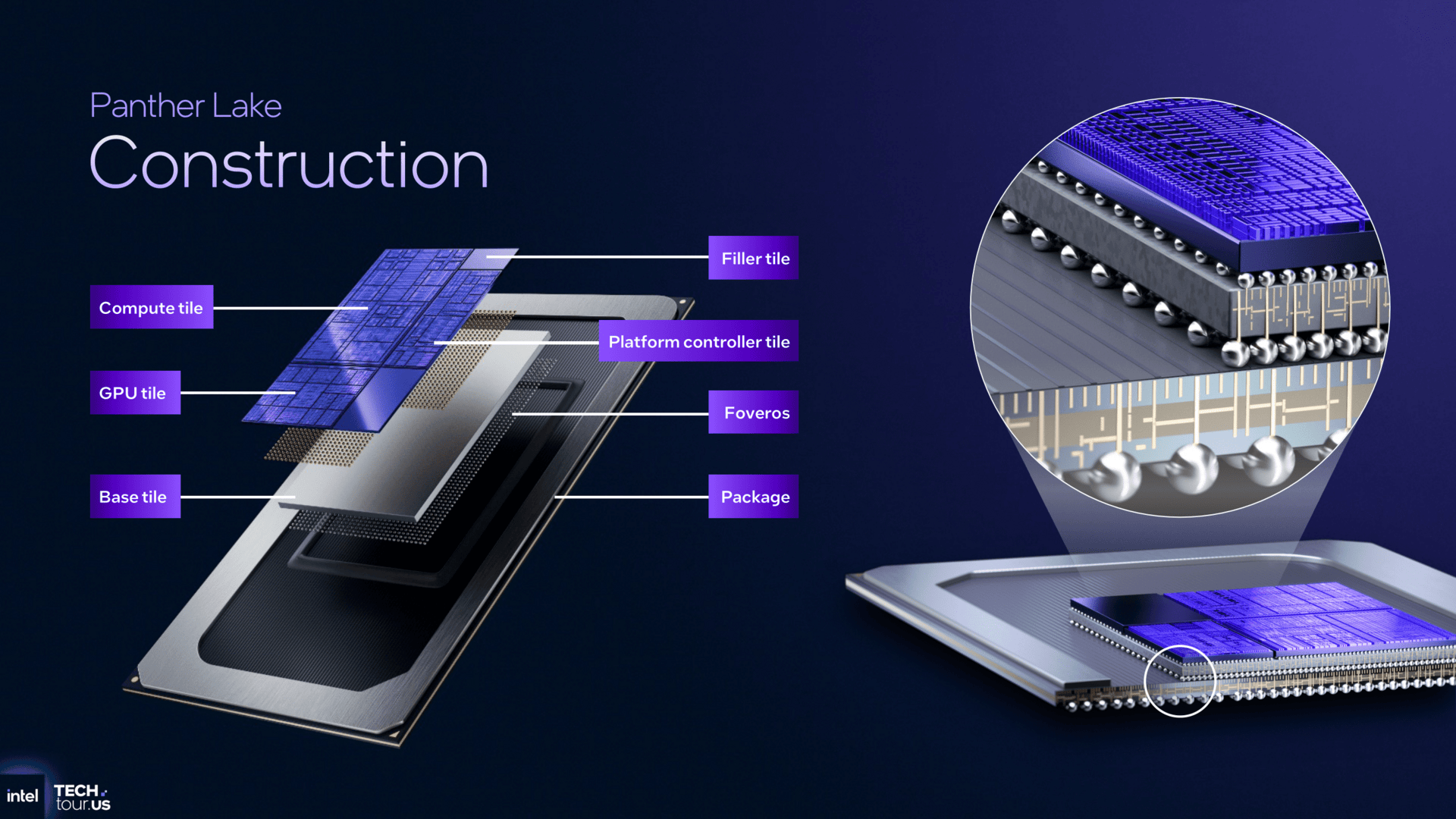
The underlying die that interconnects the components is manufactured by Intel on one of the company’s older processes. Compared to Arrow Lake and Meteor Lake, the IOE chiplet, which contained part of the connectivity, has been eliminated. This should make the design cheaper, but it is still a bit more complex than the Lunar Lake design (where there were only two chiplets, and the GPU was not separate).

The chiplet structure is allows for configurability. Both the CPU chiplets and the GPU chiplets have two variants, whose combination can create cheaper or more expensive processors. Even the IO chiplet has two variants. The chiplets are interconnected using the advanced 2.5D Foveros-S packaging.
Important design change. End of performance issues?
An important point is that in Panther Lake, the low-power LP E-Cores (derived from the E-Core architecture, but with lower clocks), which form the so-called Low Power Island, have been moved back into the CPU chiplet, just like in Lunar Lake, whereas in Meteor and Arrow Lake they were located in the SoC part. This is the part of the processor that remains active even when other parts are powered down. The LP E-Cores are not connected to the classic ring bus interconnecting the cores (and L3 cache blocks), so the ring bus and L3 cache can be powered down while the LP E-Cores handle operating system tasks or less demanding applications.

The Low Power Island is supposed to take over system operation during low loads, video playback, and idleness to improve battery life. This means that during those low-power and “standby” scenarios, the proverbial lights remains on in the CPU chiplet, instead of in the SoC part, which can be powered down. Related to this, the memory controller has also moved from the SoC or IO part into the CPU chiplet. For battery life, it’s important that it sits on the same die as the Low Power Island.
At the same time, however, being on the same die as the cores should significantly improve performance. Perhaps the biggest weakness of Meteor Lake and Arrow Lake processors is that the memory controller is in the SoC part, outside the CPU chiplet. Performance is significantly impaired because data from RAM goes to the CPU cores through two chiplets via a “D2D” interface, which adds considerable latency. In Panther Lake, these performance issues could basically disappear, if Intel implements the on-die controller and fabric properly.

Affordable models with 8 cores
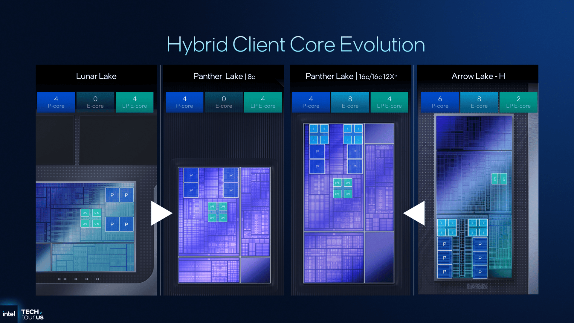
The basic, cheapest variant uses a 1.8nm chiplet with four large P-Cores, 12MB of L3 cache, and no standard E-Cores, only four low-power LP E-Cores. These are connected to the smaller of the two SoC chiplets Intel has developed which contains less PCI Express connectivity—these processors are not expected to be equipped with a dedicated graphics card. It’s possible these models will form the Panther Lake-U series (Core Ultra 300U).
These processors also get the smaller of the two versions of the integrated GPU. This is a chiplet with 4 Xe Cores, giving 512 shaders. Interestingly, this chiplet is also manufactured using Intel’s technology—the Intel 3 (3nm) process. Panther Lake introduces a new GPU architecture labeled Xe3. This is one of the biggest novelties of these processors, but we will cover it in a separate article:

Higher-performance sixteen-core models
The second, more powerful CPU chiplet contains four large P-Cores, but additionally has eight standard E-Cores added to them. In total, they have up to 18 MB of L3 cache. And in addition, there is again a quartet of LP E-Cores, making a total of 16 cores / 16 threads. This chiplet is also manufactured on Intel’s 1.8nm process. These processors would probably form the Panther Lake-H series (Core Ultra 300H), although that series will likely contain models of two types.
The first variant is intended for laptops with a dedicated GPU. This variant is equipped with the same small GPU chiplet with 512 shaders manufactured on Intel’s 3nm process as the previous cheap models (because it doesn’t need more). However, a different IO chiplet is used, which has expanded connectivity—additional PCI Express 5.0 lanes for connecting a graphics card.

Versions with a large GPU
The second alternative will be a version with powerful integrated graphics, which according to leaks might have the letter X added to its designation—perhaps before the numerical designation, so the processors would form the “Core Ultra X300H” series. It is equipped with the same more powerful CPU chiplet with 16 total cores, but is combined with a different GPU chiplet. This larger GPU is manufactured on TSMC’s 3nm process (N3E technology) and contains 12 Xe Cores—meaning 1536 shaders. Additionally, it received a large 16MB L2 cache, which will reduce dependency on memory bandwidth. It will likely be the most powerful integrated GPU in the mainstream x86 processor market, if we disregard AMD’s Strix Halo.
This variant, however, uses the smaller of the two IO chiplets, with fewer PCI Express lanes. The reason is that processor models with powerful integrated GPUs typically should not be combined with a discrete graphics card. Designing a separate IO chiplet for some processors should save a bit of the manufacturing costs per unit, but on the other hand, it means additional fixed costs for developing the second chiplet variant and procuring its tape-out and production masks.

All three processor variants, however, ultimately use the same BGA package, so any model can be installed on a single designed laptop motherboard (but to utilize the expanded PCI Express lane support in the larger IO chiplet for installing a dedicated GPU, the motherboard must be prepared for it). Manufacturers will thus be able to create laptop configurations quite flexibly.
CPU Architectures: only minor changes?
Intel stated that the P-Core architecture is named Cougar Cove. Its schematic looks practically identical to the last year’s Lion Cove architecture, and Intel does not provide any architectural data on IPC improvements (performance per 1 MHz clock speed). For now, it must therefore be assumed that the architecture is not significantly changed and Cougar Cove is primarily a port of the core to the 1.8nm process and otherwise only a slight refresh. If IPC improves, it’s probably only marginally.

Nevertheless, Intel states that Panther Lake processors will achieve higher single-threaded performance than the Core Ultra 200 Lunar Lake generation, with an improvement of up to 10% in the single-threaded SPECrate2017_int_base benchmark compared to Lunar Lake and Arrow Lake-H processors. However, note that in those, the P-Cores with the Lion Cove architecture have a maximum clock of 5.4 GHz, which is lower than in the desktop (where Arrow Lake reached up to 5.7 GHz). So for now, take the talk of increased single-thread performance with a grain of salt.

The E-Cores and LP E-Cores have the Darkmont architecture. Here too, Intel does not provide data on any potential IPC improvement compared to last year’s Skymont architecture, so we would again assume that this is only a slight refresh of the architecture, where the main point is the port to a different manufacturing process. However, Skymont was a big leap in itself, so it’s probably too soon to expect another completely new core like that.

The E-Cores are again grouped into clusters of four, in which they always share a 4MB L2 cache. While the LP E-Core clusters of Arrow Lake had reduced 2MB cache, even the LP E-Cores now have a 4MB L2 cache capacity. The standard E-Cores are connected to the ring bus and L3 cache, but the LP E-Cores are not.
SLC cache and faster memory
Panther Lake additionally has SLC (System Level Cache) memory, a system cache known from Arm processors. Intel also calls it a memory-side cache, as it is incorporated on the path to the main memory and caches data for all accesses to it—not only for the CPU cores but also for the GPU, NPU, and potentially other blocks.

Panther Lake does not yet introduce support for incoming new memory technology like LPDDR6, nor does it expand the interface (the memory has a classic 128-bit width). However, it supports faster clocks than previous processors. The version with 12 cores and the standard GPU officially supports DDR5-7200 (maximum capacity can be up to 128 GB) and LPDDR5X-8533. The version with 12 cores and the large integrated GPU, however, supports LPDDR5X-9600 (up to 96 GB maximum capacity), which provides the graphics with 153.6 GB/s of bandwidth. DDR5 memory will probably not be used with these models, to avoid harming GPU performance. The cheap models with eight cores will officially support only slower memory (LPDDR5X-6800 and DDR5-6400), but this shouldn’t be much of a disadvantage for them..
According to Intel, Panther Lake officially supports LPCAMM memory, i.e., LPDDR5X in replaceable modules. So let’s hope this standard becomes more widespread.
PCI Express 5.0, Thunderbolt 4, new wireless connectivity
There are new features in connectivity options, while some things remain the same. All Panther Lake processors, including the cheap eight-core variants, provide four USB4/ Thunderbolt 4 ports, but Thunderbolt 5 is not integrated. Furthermore, a couple of USB 3.2 ports and eight USB 2.0 ports are available.
What has improved compared to previous generations is wireless connectivity. For the first time, support for Wi-Fi 7 Release 2 and Bluetooth Core 6.0 is integrated, more precisely the digital part of the adapter is in the processor. The radio part must be added externally. All models provide this functionality, even the cheap eight-core ones. One new feature is that Bluetooth can use both of the adapter’s antennas, which improves range. Auracast technology is also newly supported.
PCI Express connectivity differs by model. Versions with the smaller IO chiplet have four PCI Express 5.0 lanes for SSDs and another eight PCI Express 4.0 lanes for other peripherals. This also applies to the models with the large iGPU. The version with the larger IO chiplet (and small iGPU), however, has 12 PCIe 5.0 lanes and 8 PCIe 4.0 lanes. The idea is thus that in a gaming laptop, the discrete GPU will be connected via PCIe 5.0 ×8 and the SSD via PCIe 5.0 ×4.
New 5th gen NPU and IPU 7.5
The NPU unit for AI applications, previously located in the SoC part, has now also moved into the CPU (Compute) chiplet. Panther Lake has a new NPU5 (5th generation) architecture with a performance of 50 TOPS in INT8 operations. It also gained support for operations with the FP8 data type. Intel switched from a design with six MAC unit engines to half the number, but with double the computational capacity in each, so the NPU now contains three engines. Overall, it should have a 40% better AI performance per unit of chip area occupied.

The IPU circuit, which serves for processing video from cameras, is also of a new generation. It enables AI-based noise removal or color mapping directly on the device (not in the cloud), supports simultaneous processing from up to three cameras, and is said to consume less power than the IPU of the previous processor generation—it’s up to 1.5 W more efficient, reportedly.
Support for 10-bit H.264, XAVC and VVC
Panther Lake also has a new media engine, and this is an area where the processor’s capabilities are among the best currently available. Only Panther Lake and its predecessor, Core Ultra 200 (“Lunar Lake”), support hardware decoding of the new VVC codec. In addition to the usual playback and compression for VP9, AV1, and HEVC formats, support for playback and compression of the 10-bit H.264 format has also been freshly added. This format is quite old by now, but practically all devices can only do hardware decoding of its 8-bit profile.
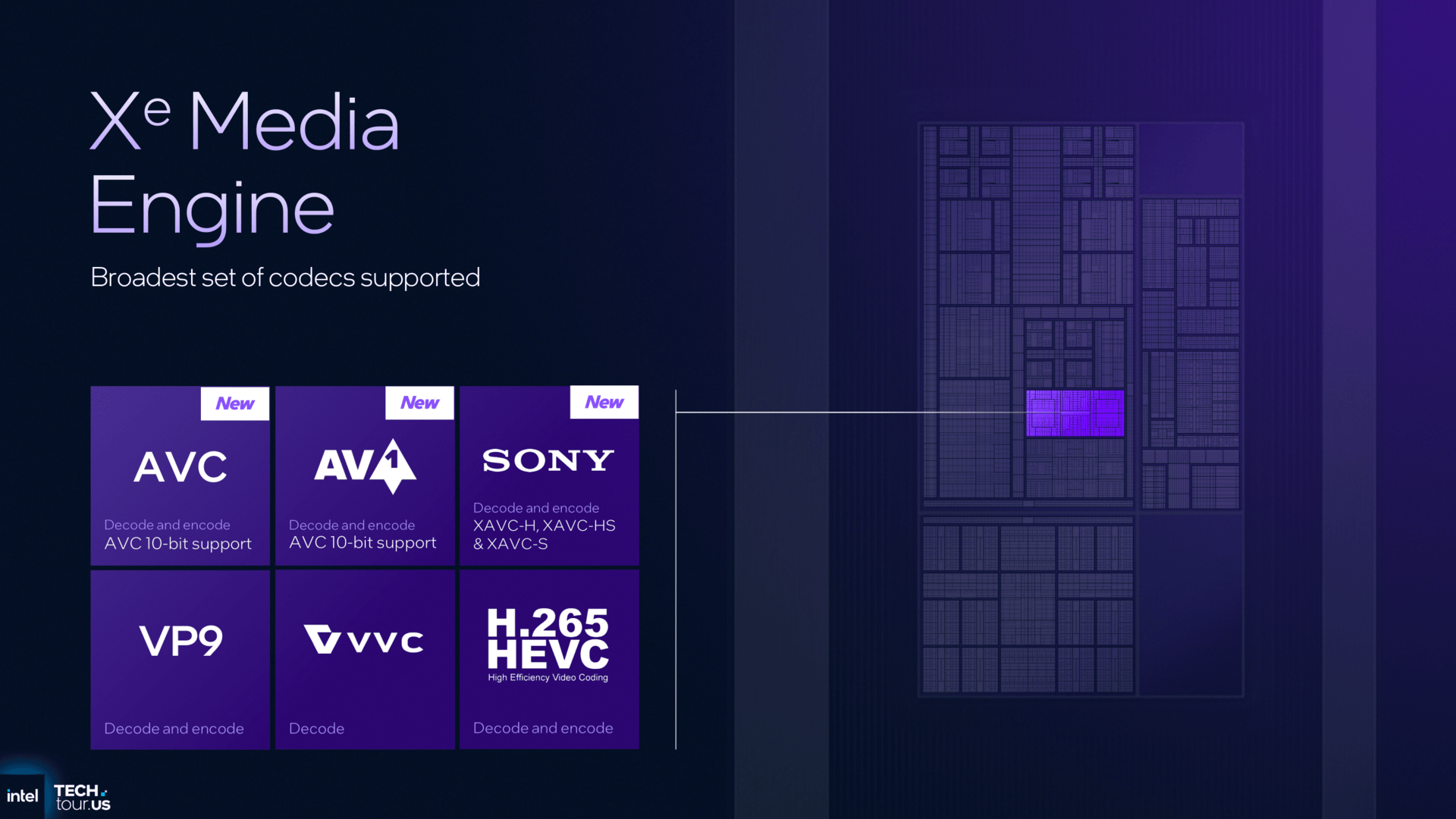
You might have seen the 10-bit H.264 profile (High 10 Profile) video used in anime content, but Intel is probably adding support for another reason. Panther Lake also adds support for he XAVC-H, XAVC-HS, and XAVC-S professional Sony video formats, which are based on top of the 10-bit H.264 format. Panther Lake’s media engine can both decode and compress into these formats.

We’ll see the results next year
So the innovations in Panther Lake processors will be mainly shine outside the CPU cores. Even though the architectures of those haven’t changed much, appearances can be deceiving and Panther Lake processors could be significantly more interesting and capable laptop platform than expected. But we will find out only next year, as mentioned at the beginning—the release is expected during CES 2026.
Sources: Intel, ComputerBase
English translation and edit by Jozef Dudáš
⠀