Intel’s chip technology has been plagued by problems over the past decade. The infamous 10nm node only became viable after years of delays and while the successor 7nm node was ultimately successful, it still came late. Since then, the company has never fully succeeded with the 4nm, 3nm, 2nm, nor with the1.8nm process which was supposed to mark a turning point. But latest reports suggest that Intel has finally managed a breakthrough.
Analysts at BlueFin Research Partners have now published a report claiming that Intel has largely—if not almost completely—resolved the yield issues that were still affecting the company’s 1.8nm technology (officially called Intel 18A) last year and during the first months of this year. Those issues likely caused the delay of Panther Lake processors (which according to earlier roadmaps were originally supposed to launch last year) as well as their limited availability after release.
According to BlueFin Research Partners, Intel has managed to eliminate most of these problems over the past few months and the technology is now fully ready for mass production while also being economically viable. This is enormously important for Intel, not only because of its 1.8nm processors (Panther Lake, Wildcat Lake, and to a lesser extent Clearwater Forest Xeon server processors), but also because the company has apparently finally managed to attract external customers to this very process node.
Intel desperately needs them to recouple the ever-increasing cost of operating its own fabs. Apple is reportedly set to trial Intel’s 1.8nm process for its M7 processors, and if Intel wants to keep Apple as a customer, it needs the process to deliver good mass-production yields.
Is PowerVia the source of the problems?
According to the same source, the previously poor yields of the 1.8nm process likely stemmed from the “wafer-to-wafer” manufacturing step. This most likely refers to PowerVia technology, also known outside of Intel as Backside Power Delivery. Instead of having the standard metal interconnect layers deposited above the silicon transistor layer (after the transistors are formed on the wafer surface) like in conventional chips, the 18A chip features two such metal interconnect stacks. The conventional stack is used only for logic signals, with power delivery wires removed, allowing higher density and improved performance. Power delivery is instead handled by a newly introduced second stack of metal layers placed beneath the transistors.
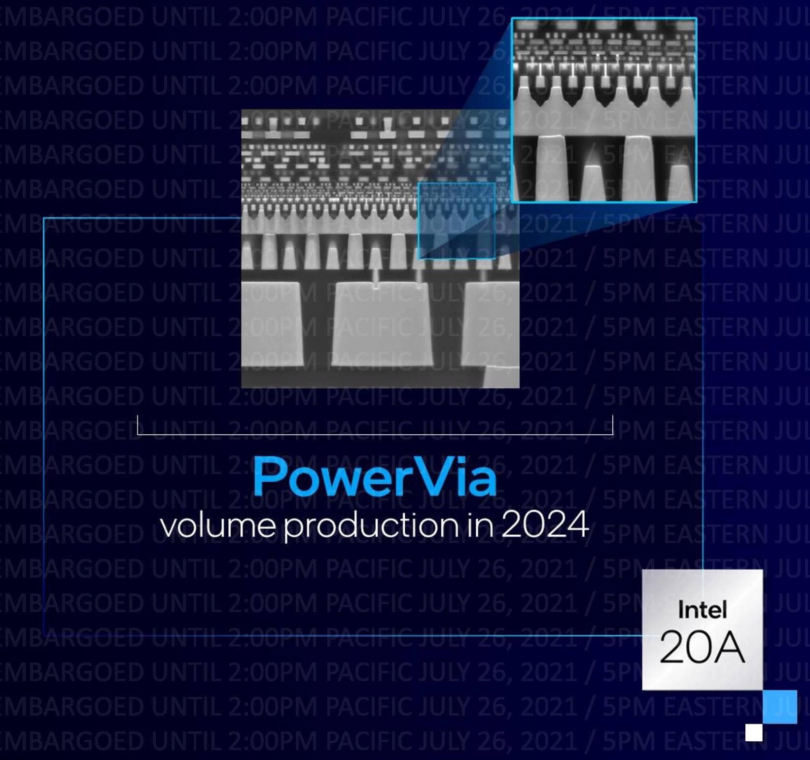
To make this possible, the wafer must be flipped (the layer order ends up inversed in the finished chip) and then thinned until the vertical Through-Silicon Vias (TSVs), which had previously been etched from the original front side, become exposed on the backside. Only then can the second stack of metal interconnect layers be built on the contact pads formed by these vias. However, to prevent the ultrathin wafer from breaking immediately and to make it possible to flip it, a protective layer and a second auxiliary silicon wafer must first be bonded to the completed front side before thinning. This temporary carrier provides structural rigidity to the heavily thinned original wafer.

This wafer handling and bonding process is new to semiconductor manufacturing, as Intel 18A is the first process to bring Backside Power Delivery into practical production. It also appears to be a highly demanding manufacturing challenge. The yield issues associated with the wafer-to-wafer process most likely resulted from flaws and defects introduced during these manufacturing steps.
Capacity should soon reach 30,000 wafers per month
Intel is also ramping up the initially limited production capacity of the 18A process. According to BlueFin Research Partners, manufacturing is now active at two fabs (Fab 52 in Arizona, while the second production line is believed to be in Oregon, likely D1X, which also serves as the company’s development facility). Both production lines are currently increasing output, with each targeting a monthly production volume of 12,000 to 15,000 wafers. This would give Intel a total 1.8nm manufacturing capacity of 24,000 to 30,000 wafers per month. For comparison, TSMC plans to reach a monthly capacity of 180,000 wafers on its 3nm process by the end of 2026.
Yield is one thing. Clock speed issues likely remain
However, the fact that the process may no longer suffer from yield problems in terms of manufacturing defects does not mean it is now entirely free of issues. Intel has also struggled with the 18A process (and previously with its 4nm technology) in another way: the chips failed to achieve particularly high clock speeds. This is evident when comparing Arrow Lake processors manufactured on TSMC’s 3nm process, which reach clock speeds of up to 5.7 GHz (the canceled Core Ultra 9 290K Plus was supposed to reach 5.8 GHz, although it is unclear whether Intel would be actually capable of yielding enough dies working at that speed), versus Panther Lake processors. Those top out at 5.1 GHz despite using roughly the same CPU core, which presumably keeps the same clock speed potential iso-process. The 600–700 MHz deficit is therefore almost certainly attributable to the 18A process itself.
This clock speed deficit is a separate issue that will not get resolved simply by eliminating manufacturing defects, so the 18A process is unlikely to achieve higher clock speeds for that reason alone. However, Intel is also preparing an enhanced version of the process called 18A-P, which is expected to improve the company’s 1.8nm technology in this regard. That should reduce the clock speed disadvantage relative to TSMC’s 3nm process. By next year, however, chips manufactured on TSMC’s 2nm process—including AMD processors—will be launching into the market, and with that, TSMC will likely once confirm the technological advantage over Intel.
According to BlueFin Research Partners, Intel has already begun so-called risk production of the 18A-P process at its D1X fab. The facility will later manufacture the 1.4nm process (Intel 14A), alongside Intel’s future Ohio fab that will serve as a second production line.
Sources: Tom’s Hardware, Jukan
English translation and edit by Jozef Dudáš
⠀