


The processor, also referred to as the central processing unit (CPU), is the most fundamental and the most important part of a computer. It is the part that executes all tasks (instructions) that are fed to the computer through program code. At the same time, peripheral devices, RAM and storage (hard drives, SSDs, oreven tape in the past) are connected to it in various ways. It is therefore truly the central element of a computer.
Now we will look at the various components that are integrated into a processor (or a SoC) today. A typical modern processor consists of a single chip in the case of a traditional “monolithic” microprocessor, but recently also of multiple chips again—these are then called chiplets, with the chiplets being parts that together form the complete functionality that would otherwise be implemented by a single chip. Intel uses the term tile for its products instead of chiplet, but the meaning is the same.
Dividing a chip into chiplets is not an outdated relic of the past, but a consequence of the fact that the increasing complexity of microprocessors is bumping against the limits of the newest manufacturing processes for chip production. This addresses such issues as the newest chip technologies being very expensive, or less suitable for implementing certain types of circuits (analog circuits and physical layers of interfaces, for example). Dividing the processor into two chiplets then allows, for example, placing the CPU cores, which benefit from the newest technology, into one chiplet manufactured by the newest leading-edge process, while placing analog functionality or functionality where performance is not critical into the second chiplet manufactured by an older mature process. Manufacturing part of the resulting area with an older chip manufacturing technology can save production costs today, because newer silicon processes may have a higher price per transistor compared to older ones (Moore’s Law postulating that prices per transistor keeps falling with new technologies, no longer applies to advanced process nodes).
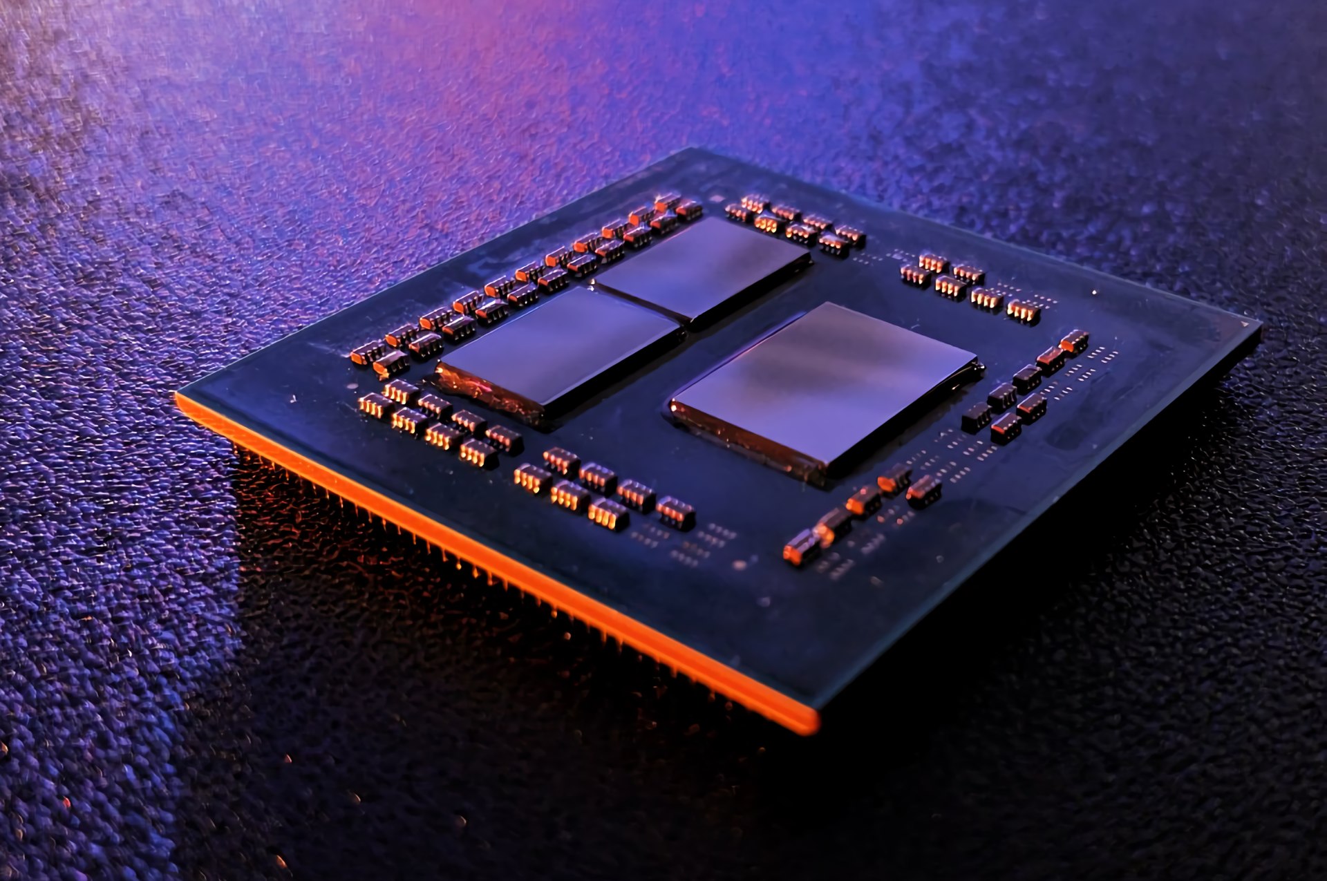
Last but not least, dividing the processor into multiple chiplets can allow for increased performance—the entire composite CPU can then have a larger silicon area than can be manufactured as a single monolithic chip (the maximum area that fabs are capable of producing chips with is given by the reticle limit, which is around 800 mm²).
Physical package
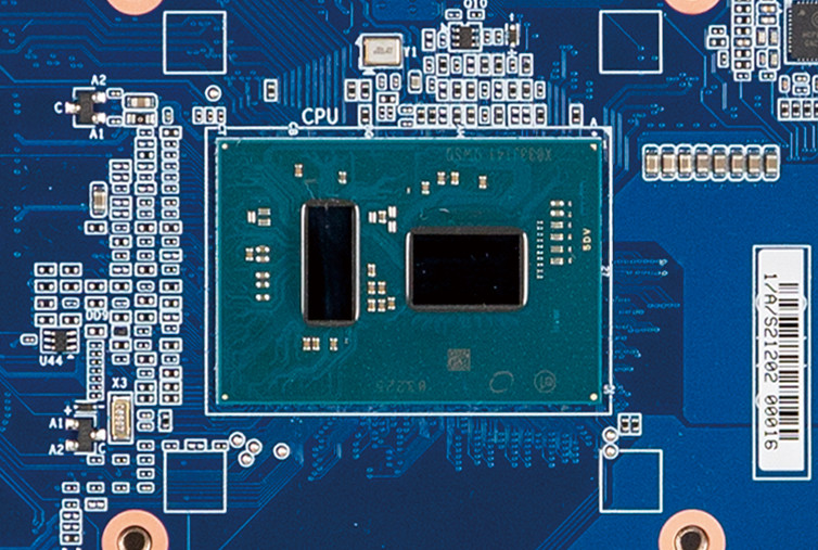
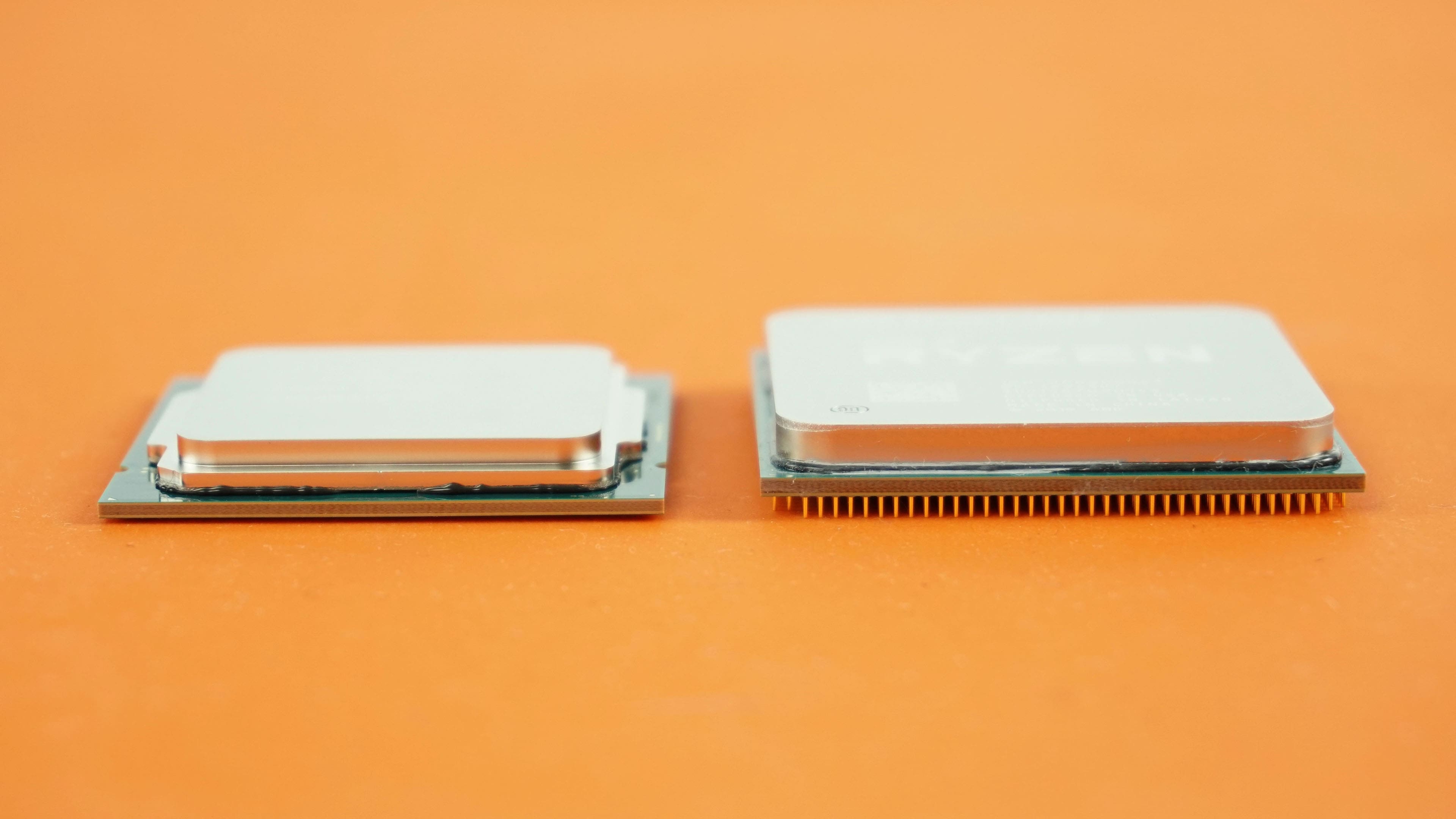
The chip or chiplets must be housed in a so-called package for use. This consists of a substrate, which is an organic printed circuit board, onto which the chip is soldered using pads on the underside of its metal layers (using the modern “flip-chip” method; before that, thin wires were instead led from the pads on the chip’s metal layers). The substrate routes electrical conductors from the chip’s metal layers themselves to the external contacts of the entire processor, which then connect to the motherboard.
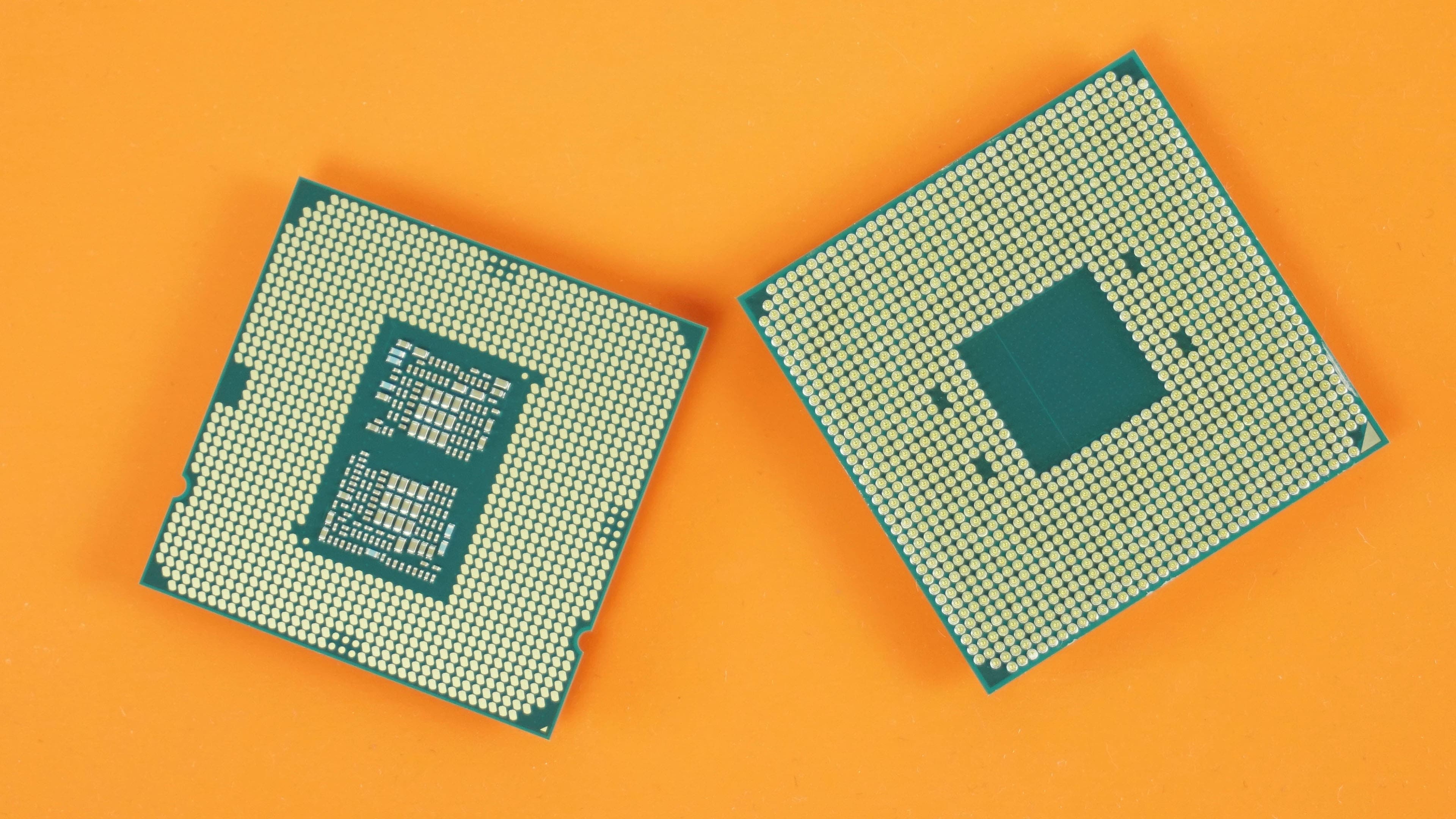
The package can be soldered directly to the motherboard—this is called a BGA type package (ball grid array, named for the solder balls applied to the contacts on the underside). In processors for desktop computers, a package intended for socket installation is often used instead, with pins on the underside of the substrate—this is a PGA package (pin grid array).
Newer processors tend to use an LGA package (land grid array), which means that there are only contact pads on the underside of the substrate and the pins that will contact them are in the motherboard socket. PGA and LGA packages allow for easy processor replacement even by the end users themselves.
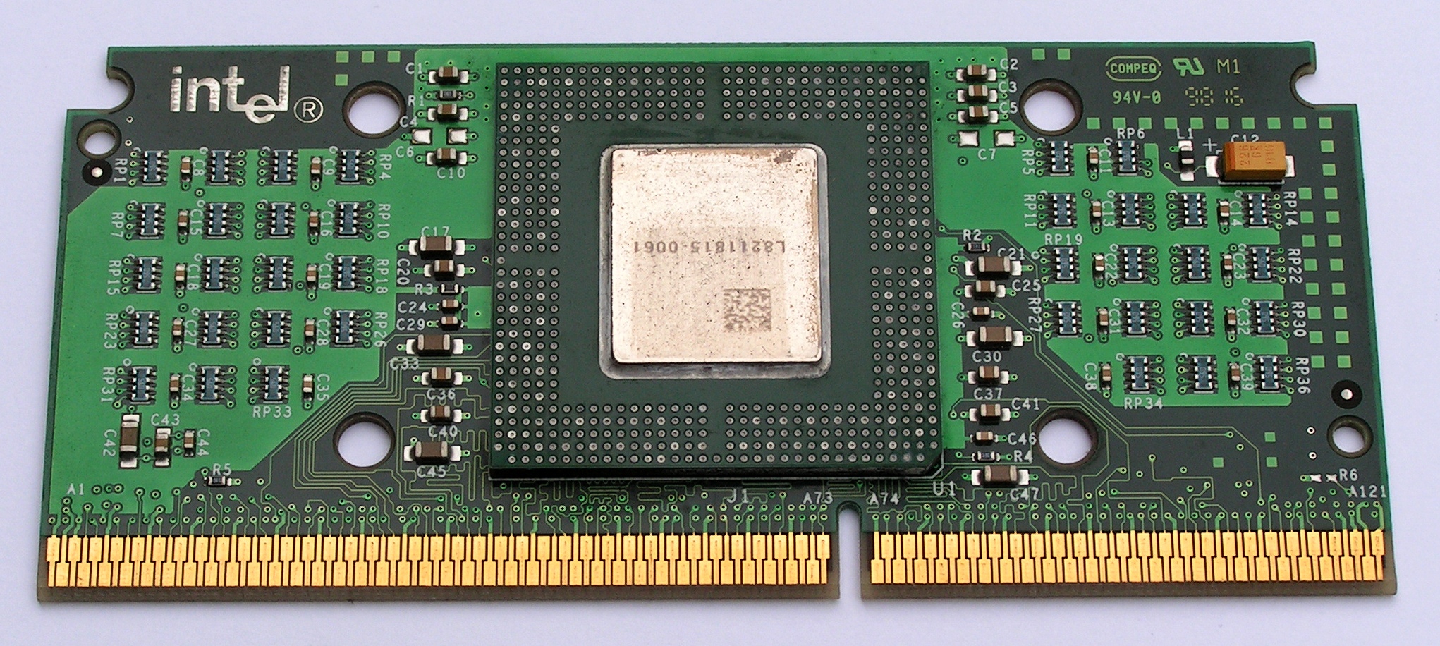
Historical microprocessors could also have simpler packages, for example DIP (dual inline package), which is a package with two rows of pins on the sides, from which the colloquial designation of chips as “bugs” is derived. Some historical processors came in a slot form factor similar to an expansion card (Slot 1 for Intel Pentium II and III processors, Slot A for AMD Athlon processors). In this case, it was essentially a processor in a BGA package, soldered onto another printed circuit board, on which there could be additional chips—particularly external cache (L2 cache) chips.
Heat spreaders and protective features
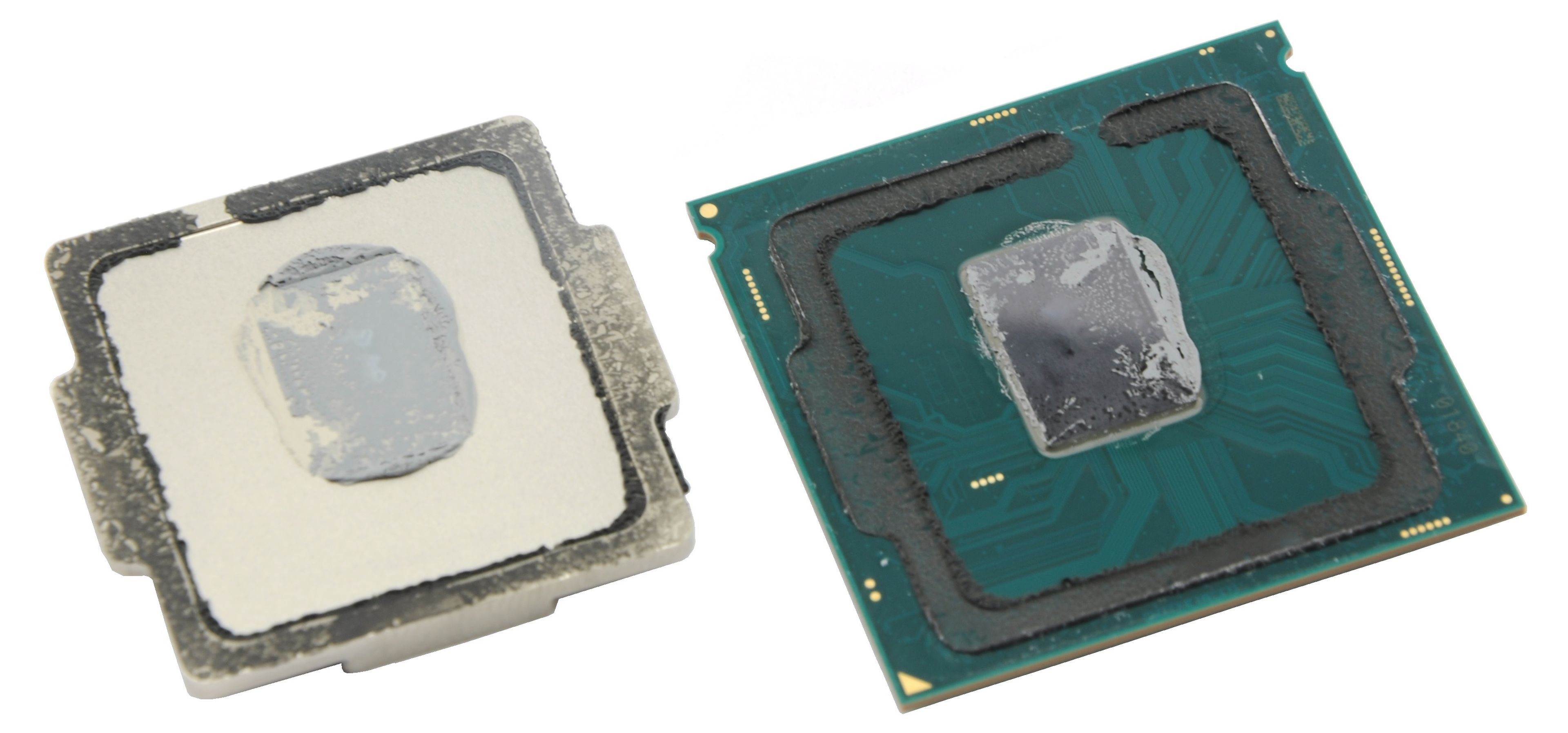
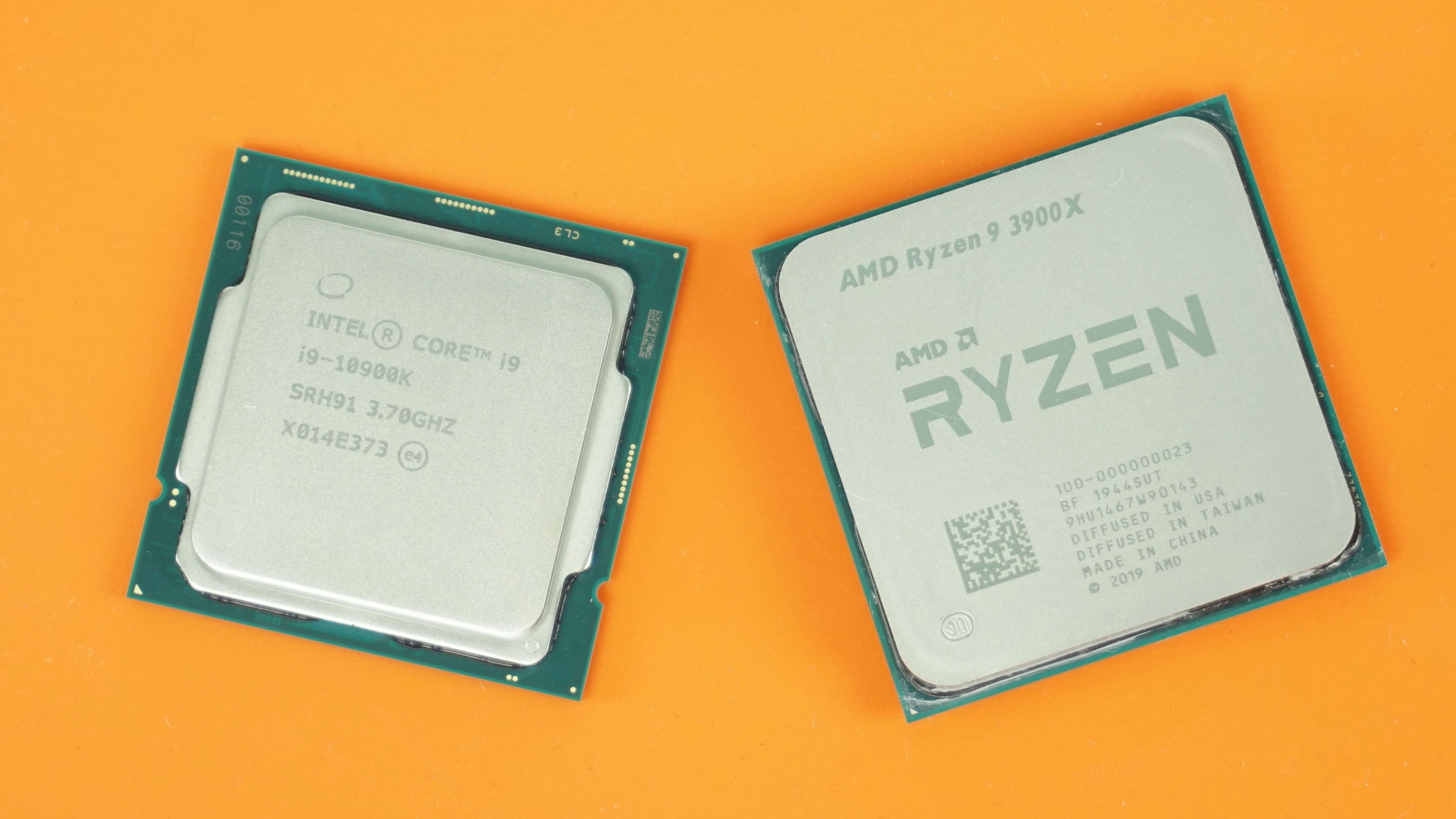
Desktop processors usually have the chip on the substrate covered by a metal lid called an integrated heat spreader (IHS). This name comes from the fact that the top surface of the IHS is significantly larger than the surface of the chip itself, so it transfers heat to the heatsink base mounted on the processor through a larger contact area. However, this IHS also provides the fragile chip with protection against mechanical damage, for example from uneven heatsink pressure. The disadvantage is that the IHS layer hampers (slows down) heat dissipation from the chip to the heatsink somewhat. Laptop processors often lack an IHS and instead use a metal frame around the processor to ensure uniform and safe heatsink mounting on the silicon.
Practically all processors for personal computers necessarily require a heatsink for their operation, because their work converts electricity into heat and the thermal output (in watts) is typically much higher than what could be safely dissipated into the surrounding environment. The processor must therefore be cooled to prevent overheating and destruction. The value of thermal output (power consumption) that the processor requires to be cooled is given as TDP (Thermal Design Power). The cooling used must be capable of dissipating at least the specified TDP of the processor, or ideally a higher value.
Thermal interface material (thermal grease, or liquid metal solution) or a special thermal pad must be applied between the IHS and the heatsink base to improve heat dissipation. The processor itself already has thermal grease or a soldered joint between its silicon chip and the IHS added during manufacturing.
The article continues on the next page…
⠀⠀


If anything doesn’t seem factually correct to you, please let us know—either in the comments or by email at info@hwcooling.net. I’ll forward everything to the author. The goal is to make sure that everything in the article is correct.