

Although Nvidia’s graphics cards of the new generation – the GeForce RTX 5090 and RTX 5080 – won’t be out until the 30th, the embargo is over and the first reviews of the top-of-the-line RTX 5090, which we also tested, are out. In this article, we take a look at the Blackwell architecture that powers these new GPUs, and its new features and functions. From DLSS 4, through compute unit architecture and chip features, to the software side of this new generation.
SMs and shaders
As before, each SM block contains 128 “shaders”, 512KB total SRAM of register file, and 128KB of L1 cache (also usable as shared memory). Nvidia often (inaccurately) refers to these shaders or shader units as “CUDA cores”, but in reality, within a GPU, the unit that corresponds to a single “core” is the entire SM block, while the individual so-called shader units are actually “lanes” of SIMD units within that core.
In this new architecture, Nvidia has changed the capabilities of the shader units. Previously, half (64) of the units were capable of calculating standard floating-point (FP) operations, which are the “bread and butter” of GPU graphics applications, while the other half, added since the Turing generation, could handle additional integer (INT) operations. Starting with the Ampere generation, this second set of units was generalized and can handle both INT and FP operations.
Now, Nvidia has extended the same capabilities to the first half of the units as well, meaning that all shaders can now process either INT or FP operations (but not both simultaneously). The performance in pure FP32 operations remains unchanged. A performance increase could occur if the running code contains more than 50 % of integer operations (which is less than typical), or the performance could improve locally at least in sections of code where INT operations dominate.

These 128 shaders are the standard units supporting 32-bit precision (FP32). Separately, within each SM block, there are also units for double-precision calculations (FP64), but there are only two of them (compared to 128 FP32/INT32 units). As a result, the GPU can process FP64 operations at only 1/64th of its full FP32 performance – this capability is essentially included just for compatibility so that code containing FP64 ops runs correctly.
Improved Shader Execution Reordering
In addition, the shaders of the Blackwell architecture feature improved dynamic ordering of the shader instruction (SER 2.0, or Shader Execution Reordering 2.0) compared to the Ada Lovelace architecture. The logic responsible for dynamically reordering operations is said to be up to 2× more efficient (though it’s hard to say exactly how this is measured). SER 2.0 is expected to have lower overhead and a better ability to identify opportunities for performance improvements.

This SER capability is not active globally at all times; by default, the GPU does not use it, so it is not something entirely equivalent to out-of-order execution in CPUs. Nvidia states that game developers can optionally enable SER via an API. It seems that SER may not always have a positive impact on performance, so the use of this technology is “opt-in”. Developers can apply it to functions where profiling indicates that SER will improve performance. So far, the adoption of this technology in games does not appear to be widespread (although it was already introduced in the GeForce RTX 4000 series), with Nvidia noting that the feature is currently used in “several ray-traced games” (indicating relatively limited number of titles).
Neural shaders
A new feature of the shaders in the Blackwell architecture is compatibility with so-called Neural Shaders. These are operations using Tensor Cores, but not targetting them as a stand-alone unit, but calling them from within shader programs that are running on shaders in a SMs. What this does is calling a pre-trained neural network with a relatively small model directly within the shader program.
This was not possible before because Tensor Cores were not tightly-enough integrated with the shader units. This capability is only now available in the Blackwell GPU architecture (note: this might not be an issue for AMD architectures, as their current form of AI acceleration is integrated into traditional compute units using the same working registers. Using both traditional shader instructions and WMMA instructions for AI acceleration within a single shader program is likely possible automatically on RDNA 3 and newer GPUs – though it’s unclear whether this approach will stay in future UDNA architectures).
Stochastic Texture Filtering
Nvidia has proposed a technique called Stochastic Texture Filtering for Blackwell, which serves as a partial replacement for more complex filtering methods (such as trilinear or anisotropic filtering) and relies on the principle of partially randomizing the result. Adding noise can help prevent artifacts like moiré patterns. For this technique, Blackwell has doubled the performance of unfiltered (nearest-neighbor) interpolation in its texture units. In this context it’s interesting that the AMD RDNA 3.5 architecture (and possibly RDNA 4 as well) has added support for accelerating unfiltered interpolation during texturing as well, in theory also targetting this stochastic filtering approach.
New Tensor Cores: FP6 and FP4 support
Tensor Cores are now in their fifth generation, and their new architecture introduces support for FP4 precision operations. This allows for double the number of operations compared to calculations with 8-bit precision (INT8 or FP8). At the same time, storing data for a model with a certain number of parameters requires only half the memory capacity compared to a model with 8-bit precision.However, the downside is the extremely low precision of these values – or rather, it’s questionable whether we can even talk about precision in this context. FP4 is supposed to allocate only two bits (i.e., four possible values) for the exponent and one bit (i.e., two values) for the mantissa, with the fourth bit being the sign. However, it seems that for AI applications, a format with a 3-bit exponent and no mantissa is also being proposed. The base would still be two, these are still binary floating-point numbers. Perhaps such data types might be better understood as something bordering between classic variable storing numbers and something which is akin to a more expressive upgrade of a true/false logical value (which is a 1-bit value).
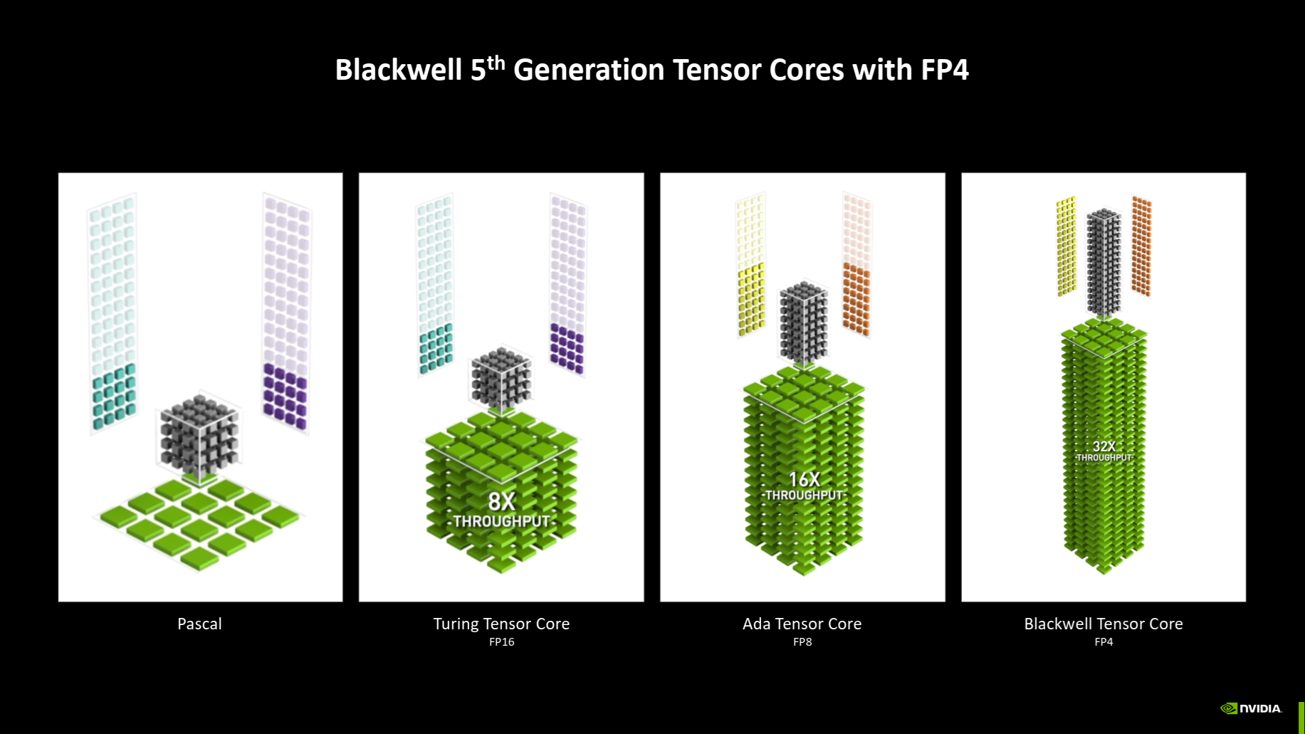
Neural networks (AI models) are generally surprisingly resistant to low-precision data – at least during inference – compared to the precision required for general-purpose numerical calculations. However, a degradation in quality of the inference results is often observed already with INT8/FP8 models, and this effect is likely to be even more pronounced with INT4 or FP4. An FP4 model with the same number of parameters would probably deliver worse results than a FP8 model. Therefore, it’s possible that the use of these low-precision values will be limited to specific applications or will require various accommodations (for example, using 4-bit precision only for part of the calculations or by increasing the number of parameters in the model). Thus, the doubling of performance may not be always achieved.
As mentioned, the ability to fit a model with a certain number of parameters into a GPU with smaller memory (e.g., 32 GB instead of 64 GB) using 4-bit values could be significant. However, the trade-off of lower quality will always be present, so it’s unclear how practical this compromise will be in real-world scenarios. An alternative to FP4 could be the FP6 data type, which Blackwell also supports for the first time. With FP6, the performance doubling likely won’t apply, and its purpose is presumably just the memory footprint savings.
On the software side, the Tensor Cores in Blackwell’s gaming chips are designed to support the same type of neural networks (which Nvidia calls the second-generation transformer engine) as the server version of Blackwell, the GB200.
RT cores with 2× compute capability
The RT cores (one in each SM block) in Blackwell GPUs are now in their fourth generation. Their main new feature is a doubled capacity for processing ray-triangle intersections (calculating where rays intersect with triangles in a scene) per clock cycle. In Ada Lovelace, an RT core was capable of handling 4 intersections per cycle, so Blackwell should be able to handle 8 intersections per cycle.

The number of intersections of rays and BVH boxes that can be processed is not specified, nor is any improvement in this area mentioned. However, the latter could still occur, because with Ada Lovelace, as far as we know four per cycle were also supported, and it’s odd that fewer operations would be supported at the BVH box (an auxiliary structure used just for the analysis) level than with the triangles themselves.
The article continues on the next page.
⠀⠀⠀